Polycrystalline Silicon Thin Films
Overview
Thin films of polycrystalline silicon, commonly called polysilicon, have many applications in integrated circuit structures. Heavily doped polysilicon and poly-silicide films have been used as gate electrodes and interconnects in MOS devices (albeit largely replaced by metal in the modern devices). Heavily doped polysilicon has also been employed for the emitter in bipolar junction transistors. More lightly doped polysilicon has been used to fabricate polysilicon diodes for use as high value resistors and as trench refill in dielectric isolation technologies. Polysilicon films have also found use in trench capacitor fabrication. Outside of the area of integrated circuit manufacturing, polysilicon films are critical to the commercial photovoltaic (PV) industry. Most of the available commercial PV panels are based on polysilicon technology.
Polysilicon thin films are produced using a process known as chemical vapor deposition or CVD. We will discuss this methodology in more detail in Section B, Chapter V, but for now, it is sufficient to know the basics of the process. In a CVD process, the substrate upon which a thin film is to be deposited (i.e., an in-process silicon wafer) is placed in a sealed deposition chamber and heated to a specified temperature. Depending on the thin film process (i.e., polysilicon, silicon dioxide, silicon nitride, etc.) and the nature of the CVD process (i.e., thermal low pressure, high pressure CVD, or plasma enhanced CVD) the deposition temperature can range between 300°C and 800°C. The process is most often carried out under vacuum conditions, but atmospheric pressure CVD process can also be employed. Once the substrate is at temperature and a clean ambient (either vacuum or inert atmosphere) has been established, a continuous and controlled flow of a gaseous precursor containing the elements needed to form the thin film is introduced to the deposition chamber. These gas-phase compounds adsorb on the hot surface of the substrate where they undergo decomposition to produce the desired solid thin film and a gaseous by-product that is pumped or purged out of the chamber. In this way amorphous (no crystal ordering) and polycrystalline thin films can be formed in the device manufacturing process.
Material and Electrical Properties
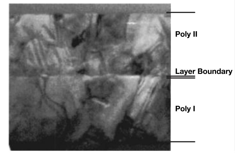
Polycrystalline silicon films are composed of domains of small (typically about 0.1 .m) microcrystals of silicon, commonly called grains, separated by grain boundaries. Figure 1 shows a transmission electron micrograph (TEM) cross-section of a polysilicon film on a silicon substrate. In TEM images, crystalline material with different crystal planes show up as having different levels of contrast in the image (i.e., some orientations will appear light, some dark). This is because different crystal planes have different atomic densities which directly impacts the intensity of the TEM image. The TEM in Figure 1 clearly shows the kind of contrast differences that indicate polycrystalline material. The many areas of differing contrast show that the film is composed of many individual crystalline domains with their crystal facets oriented more or less randomly. Note that there is some tendency towards less-than-random grain orientation in most polysilicon films since substrate characteristics can influence the crystal growth direction of individual grains.
Since polycrystalline silicon is actually made up of small domains containing crystalline silicon, it is perhaps unsurprising that many of the materials properties of polysilicon thin films approximate those of bulk crystalline silicon. Table 1 provides a comparison of a few representative properties. It can be seen that properties that depend primarily on the average value of that property in either the bulk or the microcrystals within the thin film, i.e., density and thermal coefficient of expansion, have similar values in both bulk crystalline silicon and in polycrystalline silicon films. However, properties such as the temperature coefficient of electrical resistance that are influenced by the polycrystalline nature of polysilicon thin films and by the properties of the grain boundaries are significantly different. Additionally, thin films deposited on different substrates possess unique properties such as intrinsic stress that are not relevant to bulk crystalline silicon.
| Property | Bulk Crystalline Silicon | Polycrystalline Si |
|---|---|---|
| Thin Film Density | 2.329 g/cm3 | 2.3 g/cm3 |
| Thermal Coefficient of Expansion | 2.6 µm/(m·K) (at 25°C) | 2 µm/(m·K) (at 25°C) |
| Temperature Coefficient of Resistance | -70 x 10-3 /°C | 1 x 10⁻³ /°C |
| Intrinsic Stress | N/A | Compressive: 1-5 x 10⁹ dynes/cm3 |
Table 1. A comparison of some selected properties for bulk single crystal silicon and polycrystalline silicon thin films.
The primary origins for the differences between the properties of bulk crystal silicon and polycrystalline silicon thin films are the influences of intentional doping and of the grain boundaries present in polysilicon thin films. The influence of doping on semiconductor electrical properties (and hence on the electrical properties of individual grains in a polysilicon film) was discussed in the earlier section on semiconductor physics and does not need to be repeated here. In this section we will focus on describing the impact that grain boundaries have on polysilicon thin film properties. Grain boundary regions are composed of disordered, amorphous silicon that contains many structural defects and partially bonded silicon atoms. These crystalline and chemical defects in the grain boundaries affect the resistance to electrical current flow between the silicon microcrystals and can also influence dopant distribution within the individual microcrystals. These influences have a strong impact on the electrical properties of the polysilicon film, changing their values relative to those observed for bulk, crystalline silicon.
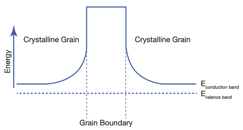
Doped polysilicon films exhibit higher electrical resistivities than bulk monocrystalline silicon that has been doped to a similar level. This is due to the combined effect of high resistivity in the grain boundaries and thermally induced dopant segregation out of the microcrystals and into the grain boundaries. Resistivity within a grain boundary is relatively high due to the fact that grain boundaries, being amorphous, have high concentrations of chemical defects. Incomplete chemical bonds in a grain boundary act as traps for charge carriers, reducing their average concentration over the breadth of the thin film and therefore increasing the effective resistivity of the film as a whole. Figure 2 shows a representation of the energy band characteristics at a grain boundary that portrays the energy band characteristics experienced by free charge carriers transiting a grain boundary. Grain boundaries are typically 5 to 10.10-8 cm wide and can be modeled as separate, amorphous silicon regions with an increased band gap.
The diffusion constants for dopant atoms (i.e., how fast a dopant atom will move through a material at a given temperature) are significantly higher in the grain boundaries than in the crystalline regions and this means that, at elevated temperatures, dopant atoms move more quickly through grain boundaries than they do through crystalline regions. Therefore, dopant atoms within a microcrystal that move into the grain boundary are transported away from that boundary faster than dopant atoms within the crystal can move to maintain a uniform concentration. This sets up a driving force for dopant migration out of the crystal that can produce relatively low dopant concentrations at the edge of the microcrystals. Phosphorus and arsenic, especially, are prone to migrate out of the crystalline grains to the grain boundaries. This phenomenon increases the average resistivity of the polysilicon film since dopant atoms that lie within the grain boundary are not effective in reducing electrical resistivity. This characteristic can present significant problems when trying to control dopant concentrations in polysilicon films at levels below saturation.
Consideration of the influence of grain boundaries on resistivity as described above can help us to understand the relationship between polysilicon film structure and electrical resistivity. Films with large grain sizes should exhibit lower electrical resistivity than films with small grain sizes, at comparable doping levels. This is due to the fact that grain boundary densities in thin film are reduced when the grain size is larger, and this leads to a relative reduction in the impact of dopant segregation and charge carrier trapping effects due to grain boundaries. In addition, grain size and dopant concentrations interact to determine the degree of dopant depletion arising from grain boundary effects. Under the influence of heat treatment, small grains with lower transit distances to nearby grain boundaries become depleted of dopants more quickly than do larger grains. This effect can be counteracted to some degree by higher dopant concentrations, since this results in narrower depletion regions that make full depletion of the grains more difficult.
Deposition of Polycrystalline Silicon Thin Films
CVD polysilicon process requires high purity, gaseous source materials that contain the silicon to be deposited. Typically, this source material is the chemical compound silane, SiH4, but some polysilicon processes have been developed that use a related silicon hydride, disilane, Si2H6. It is instructive to consider the purity requirements for CVD source gases. You may often hear the term "five nines purity" or something similar in discussions of the source gases used for CVD processes. This means that the gas must be 99.999% pure, a purity typical of electronic grade silane. Put another way, the maximum total impurity concentration permitted for CVD gases is one part in 100,000 or 10 ppm. The magnitude of 1 ppm can be understood using the following real-world comparison:
- 1 ppm = 1 oz. of salt in 62,500 lb. of sugar
- 1 ppm = 1 oz. of sand in 3 tons of concrete
- 1 ppm = 1 inch in 16 miles
- 1 ppm = 1 minute in 1.9 year
A review of some of the physical properties of silicon hydrides is provided in Table 2.
| SiH4 | Si2H6 | Si3H8 | n-Si4H10 | |
|---|---|---|---|---|
| Melting Point (°C) | -185 | -132.5 | -117.4 | -85 |
| Boiling Point (°C) | -111.9 | -14.5 | 52.9 | 107 |
| Density at M.P. (g/cc) | 0.68 | 0.69 | 0.725 | 0.825 |
| Vapor Pressure (mm) | 530 (@ -118°C) | 1 (@ -118°C) | 95 (@ 0°C) | 25 (@ 20°C) |
| Heat of Formation (kJ/mol) | +34.31 | +75 | +121 |
Table 2. Selected physical properties of some silicon hydrides.
Of the silicon hydrides shown in Table 2, only silane and disilane are indefinitely stable at 25°C and they are the primary, commercially available silicon hydrides used for CVD polysilicon processes (tri- and tetrasilane, Si3H8 and Si4H10, respectively, are available as specialty chemicals). Silane and disilane are supplied as high pressure compressed gases and it is important to be aware of safe handling procedures for high pressure compressed gases. There are a number of videos available on the web that can provide basic instructions for the safe handling of compressed gas cylinders. All silicon hydrides are pyrophoric - meaning they will spontaneously burst into flames (or explode) if they are exposed to air, which makes working with these materials particularly hazardous. Silane and disilane are thus doubly dangerous and special training is needed for anyone who regularly deals with these materials.
Polysilicon thin films are most often deposited using surface pyrolysis of silane (pyrolysis: chemical decomposition produced by heating) according to the chemical reaction sequence:
SiH4 (gas) + surface site SiH4 (adsorbed)
SiH4 (adsorbed) SiH2 (adsorbed) + H2 (gas)
SiH2 (adsorbed) Si (solid) + H2 (gas)
The overall reaction can be written as:
SiH4 (gas) Si (solid) + 2H2 (gas)
This reaction is most often performed under vacuum conditions (in a process known as low pressure chemical vapor deposition - LPCVD) at temperatures ranging between 580°C and 650°C.
Silane-based LPCVD polysilicon process characteristics have been studied extensively over the past three decades. The deposition rate increases with both temperature and pressure, as shown in Figure 3. Practically, silane-based LPCVD polysilicon deposition temperatures are limited to values below 650°C since silane reacts preferentially in the gas phase rather than on the substrate surface above this temperature. Too much gas phase reaction in the LPCVD process produces rough, poorly adhering films and particles that are device killers. Silane-based polysilicon processes performed at temperatures below about 580°C exhibit deposition rates that are too low to be of any practical use in device fabrication. However, disilane-based polysilicon processes have higher deposition rates at lower temperatures that allow polysilicon processes to operate down to about 500°C. It is important to understand that a mixed amorphous/polycrystalline silicon film is produced in any LPCVD polysilicon process that is carried out at temperatures below about 580°C and that full polycrystallinity is only achieved when the films are annealed well above this temperature. LPCVD polysilicon films are typically annealed at temperatures ranging between 800°C and 1000°C. The relative proportion of amorphous material in a deposited thin film is also dependent on the partial pressure of silicon-containing reactant during the deposition process. Films deposited at higher silane pressures, for example, exhibit significant amorphous silicon content up to temperatures as high as about 650°C.
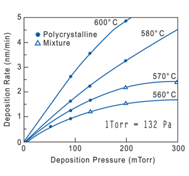 Figure 3. Deposition rate and crystallinity for silane-based LPCVD polysilicon thin films.
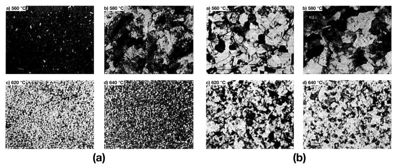
Quite complex but reasonably well-understood relationships exist between polysilicon deposition process parameters and the physical properties of the deposited polysilicon thin film. It is beyond the scope of this overview to go into great detail in reviewing these relationships, however, it is possible to give the reader an appreciation for how some of these interactions can play out. Figure 4 shows TEMs of silane-based polysilicon films in the as-deposited form. Each film was deposited at a different temperature, varying between 560°C and 640°C. The TEM analysis indicates that the films deposited at 560°C (upper left image, Figure 4(a)) are almost completely amorphous while those deposited at 640°C (lower right in Figure 4(a)) are nearly fully polycrystalline. TEM images were obtained for the same films after they had been annealed in hydrogen for 30 minutes and these are shown in Figure 4(b). While we won't go into the underlying science here, it is easy to see that the temperature of deposition has a profound effect on the crystalline characteristics of the annealed films. After annealing, the films deposited at 560°C and 580°C have much larger grain size than do the annealed film that had been deposited at 620°C and 640°C. Similar relationships are found between other aspects of the physical structure of polysilicon thin films and the deposition process pressure, the process gas flows and reaction chamber configuration.
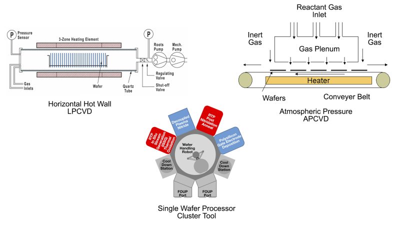
Polysilicon thin film deposition processes can be performed in batch mode, using a horizontal or vertical hot-wall LPCVD reactor, by treating one substrate at a time using a single wafer processor (SWP) or as a continuous process in an atmospheric pressure (APCVD) reactor. Basic schematics for some of the approaches to these different reactor configurations are shown in Figure 5. Each of these reactor configurations has its own unique characteristics for the deposition of polysilicon and other thin films and these characteristics will be further discussed in chapters dealing with CVD equipment. CVD encompasses many reaction-based deposition techniques which can be utilized to create thin films of desired properties. In the particular case of polysilicon CVD processes, the process characteristics directly impact the film uniformity over the substrate surface and the number of particles that are deposited on the growing film during the process. The film uniformity is determined by geometric and thermal factors unique to each CVD method. All of these parameters are varied in the development of proprietary processes aimed at achieving the ideal thin film properties for a given user’s polysilicon application.
SWP systems have gained dominance for most semiconductor CVD process requirements over the past couple of decades owing to the better control and greater production flexibility that these systems can offer. They are almost exclusively used to perform the processing steps required in advanced device fabrication.
Related Topics
Thin Films
- Silicon Based Epitaxial Thin Films
- Compund Semiconductor Epitaxial Thin Films
- Dielectric Thin Films
- Metal Thin Films
Thin Film Deposition

For additional insights into semiconductor topics like this, download our free MKS Instruments Handbook: Semiconductor Devices & Process Technology
Request a Handbook