Semiconductor Solutions
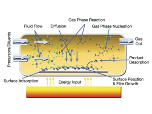
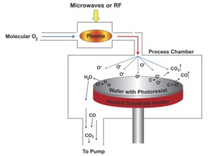
Fabricating semiconductor devices involves four broad processes: deposition, removal, patterning, and modification of electrical properties. Our solutions for semiconductors help you succeed at every step. The semiconductor industry continually faces new challenges as products become smaller, more powerful and highly mobile. Ultra-thin layers, smaller critical dimensions, new materials, 3D structures, and the ongoing need for higher yield and productivity drive the need for tighter process measurement and control.
Learn More:
MKS Handbook Second Edition
Semiconductor Devices and Process Technology
Detailing the fundamental device physics, materials, and fabrication processes used to manufacture semiconductors.
A free book from MKS
MKS Handbook
Process Technologies in Advanced Packaging
Explore the Future of Semiconductor Integration and the engineering behind Advanced Packaging – the key to sustaining Moore’s Law in the post-scaling era.
A free book from MKS
MKS Handbook
Principles & Applications in Photonics Technologies
The enabling technology for fiber optic communications, bioimaging, laser surgery, LED lighting, security, flexible electronics, wafer inspection & metrology, and lithography for semiconductor device manufacturing.
A free book from MKS
Surround the Wafer®
Our unique combination of products and services to solve the challenges of ultra-thin layers, new materials and complex 3D structures while maintaining quality and productivity.
Sensors for Improved Wafer Yield
MKS has a wide selection of process gas and instrument solutions powerful enough to ensure excellent tool optimization in Semi Fab Chambers.