Metal Thin Films for Contacts and Interconnects
Metal Materials Requirements
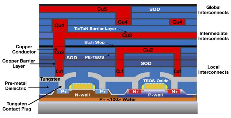
In semiconductor device fabrication, contacts are the metal components in direct contact with silicon in transistors and other devices, while interconnects are the current-carrying lines that connect discrete devices within an Integrated Circuit (IC). Figure 1 shows a cross-section of a (somewhat older) device depicting a multi-level metallization scheme. It can be seen that, within an IC structure, metals are used as gate and electrode contacts (Tungsten Silicide, light region above the source and drain), contact plugs (Tungsten Plug) and interconnects (Copper 1 through Copper 5). Diffusion limiting barrier layers (i.e. Ta and TaN) are required to prevent metal diffusion into semiconducting and insulating areas of the device.
It was noted in the section on low-k and high-k dielectrics that parasitic capacitances in metal interconnects are a cause of RC delays in signal transmission through the electrical connecting lines of an IC (the C component in RC). Of equal importance is the other parameter in this relationship, the resistance of the interconnect lines, R. For this reason, manufacturers have sought the lowest resistivity materials for interconnects in device fabrication. The electrical resistivities and conductivities of some conducting materials are shown in Table 1. It is important to note that the R component in RC delays is also reduced through the use of shorter interconnect lines. Line length reduction, along with the ability to interconnect a larger number of components per chip (packing density), have been the driving forces behind multilevel metallization in device designs. Figure 1 defines some of the terms common to this area.
| Material | Resistivity (Ω-m) | Conductivity (/Ω-m) |
|---|---|---|
| Silver, Ag | 1.59 x 10⁻⁸ | 6.29 x 10⁷ |
| Copper, Cu | 1.68 x 10⁻⁸ | 5.95 x 10⁷ |
| Gold, Au | 2.44 x 10⁻⁸ | 4.10 x 10⁷ |
| Aluminum, Al | 2.65 x 10⁻⁸ | 5.81 x 10⁷ |
| Tungsten, W | 5.6 x 10⁻⁸ | 1.79 x 10⁷ |
| Iron, Fe | 9.71 x 10⁻⁸ | 1.03 x 10⁷ |
| Platinum, Pt | 10.6 x 10⁻⁸ | 0.94 x 10⁷ |
| Lead, Pb | 22 x 10-8 | 0.45 x 10⁷ |
| Manganese, Mn | 48.2 x 10⁻⁸ | 0.21 x 10⁷ |
| Constantan (Ni, Cu) | 49 x 10-8 | 0.20 x 10⁷ |
| Mercury, Hg | 98 x 10-8 | 010 x 107 |
| Nichrome (Ni, Fe, Cr Alloy) | 100 x 10-8 | 0.10 x 10⁷ |
| Carbon (Graphite) | 3-60 x 10-5 | -- |
Table 1. Electrical resistivity and conductivity of metals at 298K.
The different metal functions within an IC have different materials property requirements. Gate and electrode contacts must provide a stable, ohmic interface between the metal conducting lines (or contact plugs) and silicon. These contacts must be able to endure the temperatures and other physical and chemical conditions experienced in post-deposition processing. Contact plugs must have highly conformal deposition processes that produce gap-free metal structures leading to a low resistance path between the electrode contacts and the interconnect network above the transistor device. Interconnects must provide a stable, high speed path for signal transfer between the device components that make up the IC.
Yves Pauleau, in a review some years ago, succinctly described the materials properties that are desirable in a metal interconnect material for use in sub-micron device fabrication:
- Low electrical resistivity
- Low resistance, ohmic contact structures
- Stable contact structures
- High electromigration resistance
- Adherence to insulating films (SiO2)
- Stable with respect to insulating films (SiO2)
- Low internal stress
- Low surface roughness
- Easily etched using plasma processes
- Fine line patternability
- Compatibility with all other semiconductor processes
- Low cost
Early on, heavily doped polysilicon and heavily doped regions in silicon substrates were used to form some of the conducting lines for integrated circuits. However, as device size shrank and speed requirements increased, the low resistivities required for contact and interconnect structures in these devices proved unachievable using doped silicon. For this reason, silicon interconnects and contacts will not be considered further in our discussion. Rather, we will discuss the elemental metal thin films now commonly employed for contact and interconnect formation. Of these, we will focus on aluminum, tungsten, and copper, along with the barrier layer materials that are normally used in conjunction with these metals. Our discussion of metal films will be conducted within the context of the material requirements listed by Pauleau.
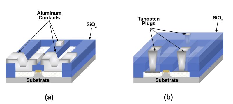
Historically, aluminum was the primary metal employed for contact and interconnect metallization in IC device fabrication. However, aluminum has been supplanted in modern devices by a combination of tungsten and copper with accompanying barrier layers such as titanium nitride and Ta/TiN stacks. Figure 2 compares some of the differences between the aluminum metallization in earlier device designs with current approaches using tungsten contact plugs prior to first level metallization.
Aluminum
Aluminum has a number of advantageous properties which led to its widespread use in earlier device generations. Aluminum metal has the third lowest resistivity of the candidate metals for metallization (Table 1). It is easily deposited as a uniform, smooth, polycrystalline film over the entire substrate surface using evaporation or sputter deposition methods (PVD). While aluminum thin films are most often deposited using PVD techniques, it is also possible to deposit aluminum films by chemical vapor deposition using volatile organometallic precursors such as triisobutylaluminum, Al(i-C4H9)3:
Al(i-C4H9)3 → Al + 3C4H8 + H2
While the CVD process has become reasonably well developed over the past few decades, most aluminum thin films for semiconductor device fabrication continue to be deposited by PVD owing to the relative simplicity and low cost of these processes. In particular, magnetron sputtering is the most commonly used process for aluminum thin film deposition due to the high deposition rates (1µm/min) achievable in this process. A key difference between CVD and PVD films has been the fact that, historically, CVD films have produced far better step coverage in high aspect ratio contact structures (CVD: 50% -100% coverage with gap fill; PVD: 15% coverage with poor gap fill). Whether deposited by PVD or CVD techniques, aluminum forms a coherent, stable film that strongly adheres to both the silicon and dielectric layers in an IC.
Once formed, aluminum thin films are readily patterned to produce contact or interconnect structures using standard photolithographic methods and chloride-based Reactive Ion Etch (RIE):
CCl4 + e- → CCl3+ + Cl* + 2e-
Al + 3Cl* → AlCl3
The aluminum trichloride produced in the RIE reaction is volatile, with a boiling point of 177.8°C, and can be easily pumped away under vacuum.
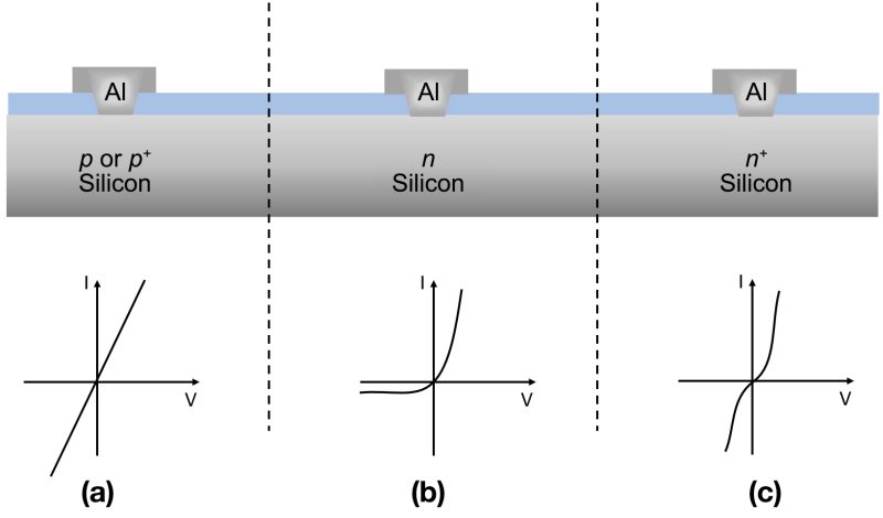
In early contact applications, aluminum was deposited directly onto silicon. It was found that, depending on the doping of the silicon, such metal contacts exhibited different electrical properties. Figure 3 shows these different electrical characteristics. Aluminum (or any other metal) in direct contact with silicon can produce ohmic, rectifying or tunneling electrical characteristics. Ideally, an aluminum-silicon contact should have ohmic characteristics, however, this only occurs when the contact is to p or p+ silicon since aluminum constitutes a p-type dopant for silicon. Aluminum contacts to n-type silicon form rectifying diodes, as described in Diode Physics. For this reason, practical contacts between aluminum (or any metal) and n-type silicon employed a thin, n+-doped region at the interface that creates a tunneling contact. While such contacts are, in fact, rectifying, when the width of the depletion layer at the metal-semiconductor interface is very thin (3 nm or less), carriers can easily tunnel across, producing the equivalent of an ohmic contact. Such barriers require n+ doping densities of 1019 cm-3 or more.
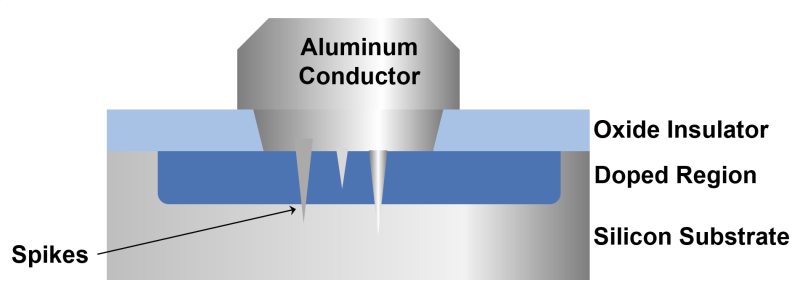
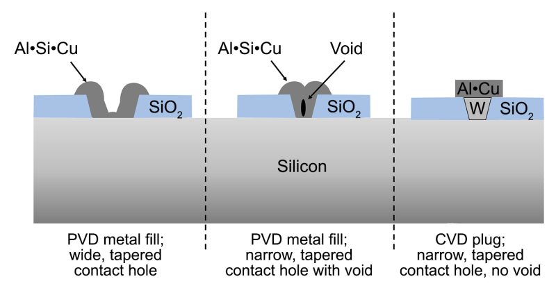
Once formed, aluminum contacts are normally annealed at high temperature (400°C) in a reducing atmosphere (forming gas; 20:1 N2:H2). This step significantly improves the contact resistance with silicon. Care must be taken that annealing temperatures remain below the Al/Si eutectic temperature since, at high enough temperatures, silicon can diffuse from the contact interface into aluminum to produce an Al/Si alloy (solubility of Si in Al at 400°C = 0.5%). When significant diffusion of silicon into the aluminum occurs, it creates voids in the silicon which are "backfilled" by the aluminum. This produces a phenomenon known as pitting or junction spiking (Figure 4). When spikes penetrate through the underlying p/n junction they can dramatically increase leakage current and/or reduce breakdown voltage. In most aluminum deposition processes, ~2% Si is added to the aluminum to prevent out-diffusion and spiking. This is another reason why PVD continues to dominate aluminum film deposition; CVD processes cannot effectively incorporate silicon into the growing aluminum film. Modern aluminum contact structures employ shallow junctions and barrier layers to eliminate rectifying behavior and prevent unintentional doping of the substrate and/or junction spiking due to metal/silicon alloy formation. In recent device generations, simple aluminum contact structures have been largely replaced by structures containing metal silicide electrodes, diffusion barrier layers and tungsten contact plugs.
Aluminum was the most common metal employed for interconnect metallization in CMOS processes above about 200 nm, however its use has been supplanted in later generations by more conductive and electromigration resistant copper metallization (see below). In addition to aluminum's higher resistance relative to other metal candidates, electromigration has been the other major issue prompting a shift away from aluminum interconnect structures. Electromigration is a phenomenon that arises from two factors:
- The kinetic influence of electron-atom collisions in the interconnect line
- The field-induced movement of ionized aluminum atoms.
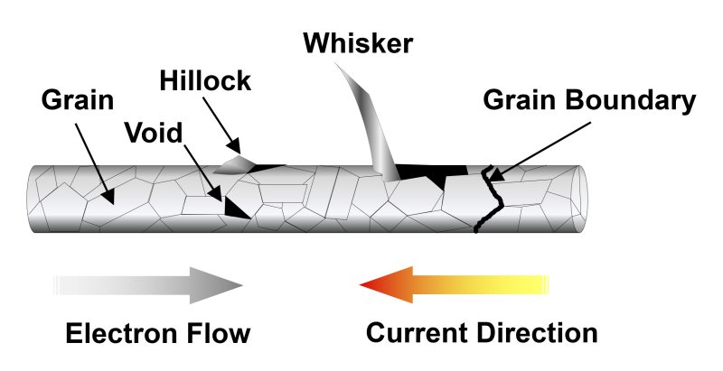
Under the influence of these two factors metal ions move toward the positive end of the conductor while vacancies move toward the negative end. The ultimate effects of electromigration are the reduction of connectivity through the creation of voids in the interconnect lines and the creation of shorts through the production of hillocks and whiskers (Figure 5). While aluminum has been largely supplanted by copper in advanced devices, those remaining applications in which aluminum is used for interconnects typically employ aluminum-copper alloys to help reduce this problem.
Tungsten
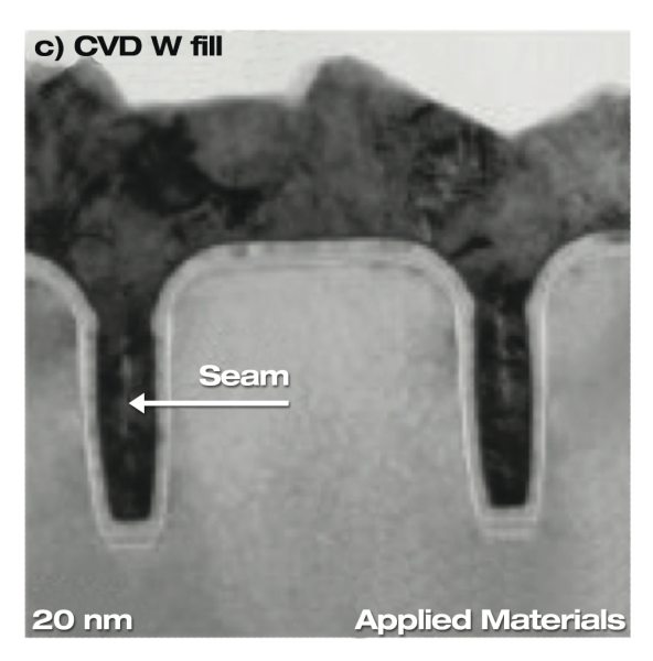
CVD tungsten, despite having somewhat higher resistivity, has replaced aluminum in contact plug applications. The use of tungsten rather than aluminum is primarily due to the better gap fill characteristics of tungsten in high aspect ratio structures (Figure 6) making it ideal for 3D-NAND. Figure 7 depicts the evolution of metal contact structures over the past few decades.
Because of its high resistivity, tungsten is employed only for plugs along with local and sometimes first level interconnects. Blanket tungsten thin films are deposited using one of the following chemical reactions:
2WF6 + 3SiH4 → 2W + 3SiF4 + 6H2
WF6 + 3H2 → W + 6HF
2WF6 + 3Si → 2W + 3SiF4
Care must normally be taken to minimize the last reaction in the above series since it can lead to the same junction spiking problems as described earlier for aluminum. For this reason, contact plugs that are fabricated using CVD tungsten processes require the use of a barrier layer, typically TiN (see below), between tungsten and silicon. More advanced device structures with very high aspect ratio contact holes employ a PVD tungsten seed layer to ensure conformal coverage by the tungsten film.
Copper
Copper has a much lower resistivity than aluminum and it has largely replaced aluminum in interconnect applications in device structures with design rules below about 200 nm. The low electrical resistivity of copper wiring greatly reduces RC delays and lowers power consumption in nanometer scale devices. Low resistivity wiring has become critical as interconnect technology has become the determining factor in signal delays on an IC chip. Additionally, copper is much more resistant to electromigration than is aluminum.
The advent of copper as an interconnect material was initially hampered by the fact that it is a highly mobile metal and thus can produce unintended contamination, both in the fab and on-chip. Furthermore, the conventional approaches to thin film deposition and etch are not possible with copper, making it difficult to create patterned structures on a device surface. Any issues associated with unintended copper contamination within the fab were fairly easily resolved by isolating copper processing areas from other fab areas. On-chip contamination presented a somewhat more difficult problem. Since copper easily migrates into both the dielectric and semiconducting materials that surround it on a device surface, diffusion of the metal could only be prevented by the total encapsulation of copper structures by barrier materials. The need for patterning copper layers on substrate surfaces eventually necessitated the development of a completely unique approach for the formation of copper interconnect structures. Finally, copper, unlike aluminum, lacks a stable, adherent native oxide and this makes it more prone to corrosion and adhesion problems in integrated device schemes. Barrier (capping) layers have been developed that alleviate this problem.
Copper can be deposited using PVD, CVD or electrochemical plating technologies. Either a physical or chemical pre-deposition clean is needed prior to the deposition of a barrier layer (see below) followed by a seed layer for copper electroplating. Practical PVD processes for copper deposition do not produce usable thicknesses for interconnect formation; they are limited to the formation of copper seed layers that promote follow-on copper electrodeposition for interconnects. PVD processes have poor step coverage and gap-fill characteristics and this makes them unsuitable for copper deposition beyond this initial seed layer. CVD processes could conceivably fulfill copper thin film needs. However, the available volatile precursors for copper CVD processes are very limited. No volatile, simple, binary copper compounds similar to silicon halides or hydrides are known. Rather, copper CVD precursors are complex organometallic species that are difficult to manufacture and costly to use. Additionally, CVD copper processes tend to produce relatively impure copper films and blanket CVD copper films do not lend themselves to subtractive patterning. As a consequence of the issues with PVD and CVD copper, the primary method for depositing copper layers in semiconductor device fabrication is a unique-to-copper electroless deposition process.
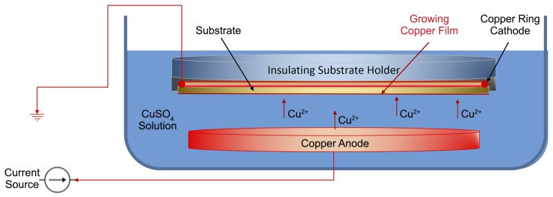
Figure 8 shows a schematic representation of the electroplating process. Electrochemical processes for copper typically use some variant on solutions containing inorganic copper salts to deposit bulk copper on a substrate surface. In electroplating processes, these solutions typically employ copper sulfate, CuSO4 and a copper anode to drive an electrochemical reduction:
Cu2+ + 2e- → Cu0
Electroless plating reactions (i.e. electrochemical processes that do not require external electrodes) are also being explored. These processes reduce copper ions to copper metal without the need for electrochemically driven reactions, for example:
Cu2+ + 2HCHO + 4OH- → Cu0 + 2HCOO- + 2 H2O + H2
The actual solution chemistries employed by different equipment/process suppliers for use in their copper deposition tools are highly proprietary. These proprietary solutions tend to be complex mixtures of inorganic copper salts with various inorganic and/or organic process promoters.
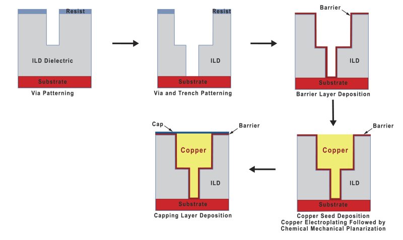
Coupled with the problems in finding viable deposition processes for copper was the fact that patterning copper films cannot be accomplished using conventional methods. Common fluoride or chloride-based dry etching technology does not work for copper since the fluoride and chloride by-products of the etching process are non-volatile and cannot be easily removed to create a patterned interconnect structure. These difficulties with the deposition and patterning of copper led, in the late 1990's, to the development of a unique copper metallization process known as the Damascene Process, shown in Figure 9. Damascene processing completely eliminated the need for the use of dry etching in patterning copper lines and vias. Rather, dry etching is performed on the dielectric material where the material is placed. Damascene processes also introduced the use of special barrier layers such as Tantalum, Tantalum Nitride, Titanium Nitride, and Titanium-Tungsten that prevented copper diffusion into other materials in the IC and improved the adhesion of the subsequent copper layer. Figure 49 shows a schematic for the Dual Damascene process. In this process, the interlayer dielectric is first deposited on the substrate using conventional CVD methods, then patterned using standard photolithography and dry etching techniques to produce the via pattern. Next, the trench pattern is created, again using conventional photolithography/dry etch. A barrier layer impermeable to copper diffusion is then deposited, followed by the deposition of a PVD or CVD copper seed layer. Once the seed layer is in place, the substrate undergoes a blanket copper electroplating process, filling both the vias and trenches in a single step to create the copper interconnect. Following the electroplating process, the copper on the surface of the substrate is polished back using chemical mechanical polishing, CMP. This step stops when it contacts the interlevel dielectric (ILD), leaving only the copper in the vias and trenches. The CMP process is described in more detail in the Etch Overview. Finally, a capping layer of a material impermeable to copper diffusion is deposited, resulting in complete encapsulation of the copper in the vias and trenches. Manufacturable copper process technology was first introduced by IBM and Motorola in 1997 and developments since then have made copper metallization common throughout the industry.
Barrier Layers
Barrier layers are needed as metal diffusion barriers for contact electrodes and copper capping layers. Depending on the materials and process compatibilities between the barrier layer and silicon or a particular metal, different barrier layers are preferred for different applications. However, a number of general materials properties can be identified for barrier layers, including:
- High degree of metal impermeability at sintering temperatures (sintering refers to joining of the materials by thermal means)
- Ohmic and low contact resistance
- Good electrical conductivity
- Good adhesion between the semiconductor and metal
- High electromigration resistance
- Good step coverage
- High deposition rates in high aspect ratio gaps
- Compatible with chemical-mechanical polishing (CMP)
Aluminum is no longer common in contact structures and, so, we will not consider barrier layers for aluminum in any detail. In those remaining multilevel metallization schemes that still employ aluminum, titanium nitride, TiN, is the barrier material of choice since it has a low enough resistivity that it can become the principle conductor should electromigration produce a void in an aluminum line. TiN is usually deposited by PVD methods (typically by ion plasma PVD). CVD TiN processes have also been developed that use either inorganic halide or organometallic titanium chemistries:
3TiCl4 + 7NH3 → 3TiN + 4NH4Cl + 5/2H2
Ti[N(CH3)2]4 + 4NH3 → TiN + Mixed by-products
The ammonium chloride product of the inorganic (TiCl4) route to TiN can lead to high maintenance requirements in the deposition equipment and this has produced a strong interest in organometallic CVD processes employing TDMAT (Ti[N(CH3)2]4) and similar chemical compounds. Titanium nitride is also commonly used as a barrier layer for tungsten contact plug and interconnect applications.
Barriers, liners and capping layers are an inherent part of copper metallization technology. Damascene and Dual Damascene Cu metallization processes normally employ Ta/TaN as the barrier layer for sidewalls and at the bottom of lines to prevent copper diffusion into surrounding device components. Typically, these layers are deposited using advanced PVD methods that can achieve uniform and conformal coverage in high aspect ratio vias and trench structures. Once copper metallization is in place on a device, the metal requires a top (capping) barrier to prevent corrosion of the copper and to promote adhesion between the copper and subsequent dielectric layers. Capping layers that have been developed for copper are primarily relatively high-k dielectric materials, typically silicon nitride, silicon carbon hydrogen, or silicon oxide carbide.
Related Topics
Thin Films
- Polycrystalline Silicon Thin Films
- Silicon Based Epitaxial Thin Films
- Compund Semiconductor Epitaxial Thin Films
- Dielectric Thin Films
Thin Film Deposition

For additional insights into semiconductor topics like this, download our free MKS Instruments Handbook: Semiconductor Devices & Process Technology
Request a Handbook