Low Pressure Chemical Vapor Deposition Systems
LPCVD deposition systems typically operate at pressures that range from 0.1 to 10 Torr. The reader will recall that this is considered a medium vacuum application. Reactor configurations that have been used for LPCVD thin film processes include resistance heated tubular hot-wall reactors, vertical flow batch reactors and single-wafer reactors. Throughout the latter part of the 20th Century, much LPCVD processing was performed in horizontal hot-wall tube reactors, a schematic of which is shown in Figure 1.
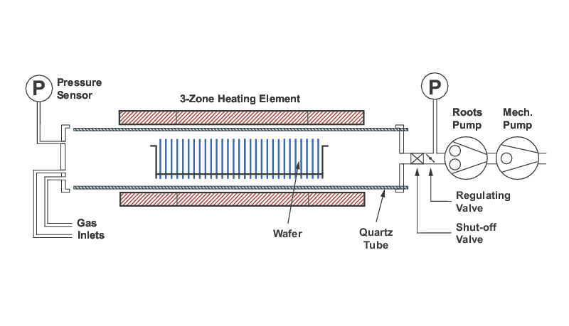
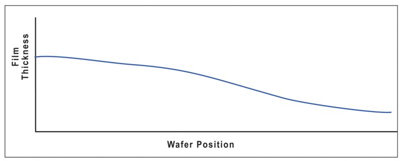
These reactors could process 100 or more wafers simultaneously and were very successful in depositing LPCVD silicon dioxide, silicon nitride and polysilicon thin films. LPCVD reactions for these films require temperatures that range from 425°C (silicon dioxide, low temperature oxide, LTO) to 740°C (silicon nitride) with occasional processes running at greater than 800¡C (silicon dioxide, high temperature oxide, HTO). These process temperatures are achieved using resistive electrical heaters. The precursor gas in this equipment configuration is fed into the reaction chamber using either an inlet at the front of the tube or long injector tubes which lie on the bottom of the tube and run the length of the boat of wafers. However, both of these gas inlet configurations present problems for the user. If the precursor is simply fed in at the front of the tube, it will react on the wafer and equipment surfaces as it passes down the tube, depleting the precursor concentration in the gas phase. This results in higher precursor concentrations and therefore thicker deposited films on wafers located at the front of the tube. As a consequence, the film thickness profile for a LPCVD process in which the precursor is input at the door and a constant temperature is maintained over the wafer load looks like that shown in Figure 2. This depletion problem could be overcome through the use of temperature ramps over the wafer load (increasing temperatures towards the pump end of the load) or through the use of gas injectors in lower temperature processes. However, as device designs grew smaller in the 1990s and early 2000s these solutions failed as they led to unacceptable variations in film properties (between films deposited at the cooler temperatures at the door end of the load and those deposited at the higher temperature pump end) or to reproducibility and costly maintenance issues in the case of injector use. Additionally, the relatively high time-at-temperature burden of batch hot-wall processes could no longer be tolerated when processing devices at smaller design rules. Finally, certain hot-wall LPCVD processes required "caged boat" wafer carriers (doped TEOS oxide, in situ doped polysilicon) that produced particle levels that were unacceptable for advanced device processing. For these and other reasons, horizontal hot wall systems have fallen into disuse in most fab environments.
The failings of conventional LPCVD equipment in advanced device processing led to an exploration of several alternative equipment configurations for LPCVD processes. Cold-wall, inductively coupled systems and cold-wall, vertical flow small batch systems experienced some acceptance and can still be found in use today. However, modern fabs have largely migrated to the use of single wafer cluster tools for CVD and other processing needs owing to demonstrated advantages in wafer handling, effective particle and process control and process integration.
Single wafer cluster tools process a single wafer at a time in small process chambers that can be designed for optimal performance in a variety of areas. Gas recirculation and surface-to-volume characteristics within single wafer chambers can be much more precisely tuned than in other equipment configurations, eliminating any potential for gas phase nucleation and in-process particle generation. Fluid flow and diffusion is much more effectively controlled in these configurations which results in more efficient use of precursors and higher deposition rates. The latter characteristics have allowed device manufacturers to significantly reduce the time-at-temperature burden in CVD processes, a key requirement in the manufacture of devices with nanoscale geometries. These and other more process-specific advantages have resulted in the wide-spread use of such cluster tools within the industry.
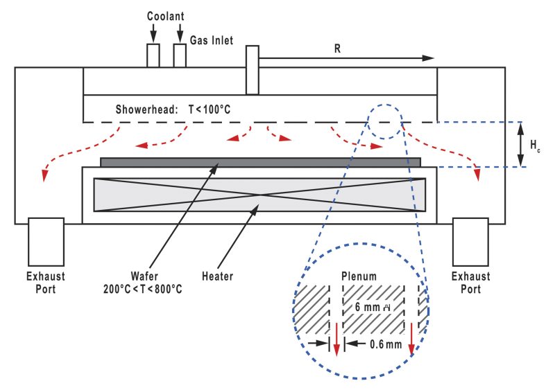
The internal configuration of a single wafer process chamber within the cluster tool depends on the intended process to be performed within the chamber. Figure 3 shows a schematic of a representative single wafer CVD chamber. Precursor is fed to the chamber using a showerhead arrangement that ensures a uniform concentration of precursor over the entire wafer face. The showerhead and chamber walls are cooled to temperatures below which deposition should not occur in order to minimize any potential for particle production by the spalling of deposits on these surfaces. The substrate is heated using resistive or optical heating of the wafer chuck. The gas exits the chamber via exhaust ports below the wafer. The geometries within the chamber are precisely designed to optimize process performance for zero particle generation, even film uniformity and desirable film properties.
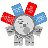
Figure 4 shows a schematic for a cluster tool configuration. Wafers are introduced into a transfer station using a load-lock arrangement and FOUP protocols. Once the transfer station has been pumped to vacuum conditions, a robotic wafer handler (in the central chamber) picks up the wafer and transfers it to a process chamber. The process chamber is sealed and the wafer undergoes the intended process, in this discussion thin film deposition by CVD. When the process is complete, the wafer is extracted from the process module and transferred either to another process module (i.e., gate stack processing, annealing, etc) or to a cooling module then to the transfer station that is brought back to atmospheric pressure so that the processed wafer can be removed from the system.
Related Topics
Thin Films
- Polycrystalline Silicon Thin Films
- Silicon Based Epitaxial Thin Films
- Compund Semiconductor Epitaxial Thin Films
- Dielectric Thin Films
- Metal Thin Films
Thin Film Deposition
For additional insights into semiconductor topics like this, download our free MKS Instruments Handbook: Semiconductor Devices & Process Technology
Request a Handbook