Compound Semiconductor Epitaxial Thin Films
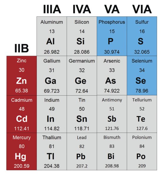
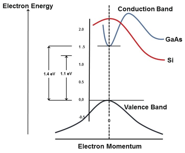
Compound semiconductors are materials such as GaAs, AlGaAs, GaN, CdSe, InP, InSb, etc. These materials combine the elements from equidistant columns on either side of Column IVA of the Periodic Table, to produce materials having the general formula ANB8-N, where the superscripts refer to the periodic group containing the element (i.e., II-VI, III-V, etc.). III-V materials, especially GaN and GaAs, along with silicon carbide, SiC, are the dominant commercial compound semiconductors and have the longest history of device usage. GaAs-based microelectronic devices, for instance, exhibit much lower signal noise than do microelectronic devices employing other types of semiconductors. This is a very important attribute in weak signal amplification. In addition, they are much more resistant to radiation-induced damage than are silicon devices. GaAs has a direct optical band gap of around 1.4 eV which allows it to be used for thin film solar cells as well as for light emitting diodes. The term "direct band gap" implies that a material emits a photon of light through a single, direct electronic transition between the valence and conduction bands of the material (Figure 2). "Indirect" band gap materials such as silicon require that an electron pass through an intermediate state during such transitions, prohibiting direct photon emission.
Device technology employing GaAs and InP substrates is reasonably well developed and these substrates are currently used in ways analogous to silicon for the fabrication of advanced electronic devices. Microelectronic device fabrication on GaAs substrates has a long history in high speed and radiation hardened military and space applications and, more recently, in commercial opto-electronic devices. InP substrates have been employed for the fabrication of optical network components such as Dense Wavelength Division Multiplexing (DWDM) lasers [84], Vertical Cavity Surface Emitting Lasers (VCSELs), pump lasers, etc. as well as for high speed electronics circuits. GaN substrates have become available and are finding use in optical device manufacture due to the fact that GaN alone offers light emission in the blue region of the spectrum (needed for white light LEDs). GaN substrates are also being used for the manufacture of power devices. Finally, silicon carbide, SiC, is being used for substrates for more efficient and compact power electronics in motor controls, power supplies and inverters.
Compound semiconductor substrates suffer from certain material properties when used in device fabrication. Heat dissipation in compound semiconductors is hampered by their much lower thermal conductivity as compared with silicon. This is a significant problem for the use of these substrates in applications with even normal power dissipation requirements. Another drawback of compound semiconductors, when compared with silicon, is that it is impossible to grow a well-behaved, strongly insulating thermal oxide on these binary and ternary compounds. Thermal oxidation of GaAs or InP (and others) results in preferential oxidation of one of the elements over the other and in the production of an oxide with poor material and electrical properties. This issue has probably been the single most important factor in limiting the use of compound semiconductor substrates since the early days of integrated circuit manufacture. Indeed, in the latter part of the 20th Century there was a standing joke within the industry that GaAs was and would always be the "material of the future" for just this reason. This being said, the advent of smaller feature size and advances in deposition methods such as Atomic Layer Deposition (ALD) has made the issues of native oxide removal and insulating oxide layer formation more easily addressable in compound semiconductor device fabrication, opening many opportunities for this technology. Epitaxial film deposition is a critical technology for leveraging the advantageous electrical properties of compound semiconductors in advanced devices and significant effort has been applied to the development of processes and equipment for this purpose.
Epitaxial methods for the deposition of thin films of compound semiconductor materials have made possible the synthesis of artificial crystal structures such as quantum wells and superlattices that have opened myriad possibilities for the use of compound semiconductors in microelectronic devices. In the past two decades, these new structures have found many applications that exploit their superior electrical and optical properties in advanced electronics, photovoltaic, optical and optoelectronic devices. Modern multiple quantum well lasers, for example, contain graded index separate confinement heterostructures (GRINSCH) or VCSEL's that emit light at very low threshold currents at room temperature under continuous wave operation.
The quality of epitaxial layers of compound semiconductors, like that of silicon epitaxial films, is critically dependent on the crystallographic characteristics of the substrate on which the layer is grown and on interfacial relationships between the substrate and epitaxial layer. As with silicon epitaxy, substrate surfaces must be clean and free of all contaminants, including any native oxide. Surface cleaning is a much more complex problem with compound semiconductors than it is with silicon, due primarily to the binary, ternary or quaternary chemistry of these surfaces. Many different approaches have been, and continue to be, evaluated for cleaning. To date, there is no universal approach for such cleans, with successful cleaning procedures being very much tied to the chemical make-up of the particular compound semiconductor and to the interfacial characteristics required in a given application. Bromine/methanol, ammonium hydroxide and hydrochloric acid based wet chemistry methods, analogous to the ammonium hydroxide and hydrofluoric acid chemistries used in silicon processing, have been used to clean GaAs surfaces for some applications. Thermal annealing methods have also proven successful in removing native oxides from compound semiconductor surfaces. Hydrogen passivated surfaces have been produced on GaAs and other compound semiconductors by methods such as atomic hydrogen cleaning utilizing remote-plasma- generated atomic hydrogen. The crystal lattice quality and orientation of the substrate also plays a critical role in the properties of epitaxial compound semiconductors since lattice mismatching between substrate and film leads to strain in both crystal lattices. Those readers seeking in-depth discussion of the issues surrounding interfacial effects in compound semiconductor devices are referred to reference.
A number of approaches have been (and continue to be) developed for producing epitaxial layers of compound semiconductors. Methods such as Liquid Phase Epitaxy (LPE), UHV-CVD, VPE, and MBE have all been successfully employed for compound semiconductor epitaxy, however, the most successful approach for industrial applications has proven to be Metal Organic Chemical Vapor Deposition, MOCVD. MOCVD is being used broadly for epitaxial layer deposition in both conventional, atmospheric pressure CVD reactors and in advanced ALD reactor configurations.
The primary advantage of MOCVD for compound semiconductor epitaxy is the fact that most of the metal constituents in these materials are available as readily transportable, commercially available, high purity organometallic compounds. Organometallics are chemical compounds that incorporate both a central metal atom and attached organic groups. They are all relatively volatile and thus they can be used to carry relevant metals, especially those in Groups II and III in the periodic table, into a reaction chamber where they decompose on the hot substrate surface, depositing the desired epitaxial film. Volatile hydrides of these metals, analogous to the common precursors for silicon (SiH4) germanium (GeH4) and dopants (B2H6, PH3) are either unknown or chemically unstable and thus unavailable for use in CVD epi processes. With the exception of gallium chloride, Ga2Cl6, halides of these metals (analogous to the chlorosilanes) are unusable in MOCVD, primarily due to the fact that they are non-volatile solids. As a result, metal organic compounds have proven the best precursors for epitaxial processes and they include compounds such as:
- trimethylgallium (TMG - Ga(CH3)3)
- triethylgallium (TEG - Ga(C2H5)3)
- trimethylindium (TMI - In(CH3)3)
- trimethylaluminum (TMA - Al(CH3)3)
- trimethylantimony (TMSb - Sb(CH3)3)
- diethylselenium (DES - Se(C2H5)2)
- dimethylcadmium (DMCd - Cd(CH3)2)
Examples of the process chemistry employed for MOCVD compound semiconductor epitaxial processes include:
Ga(CH3)3 + AsH3 + H2 → GaAs + CH4 + H2
Cd(CH3)2 + Te(i-C3H7)2 + H2 → CdTe + CH4 + i-C3H8
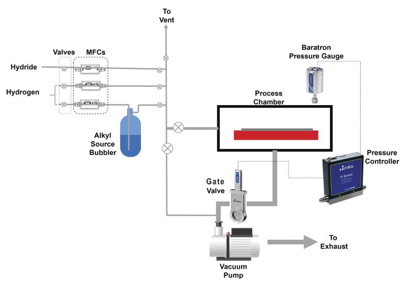
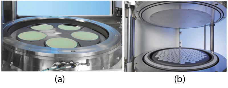
As in Si and Si1-xGex epitaxial processes, MOCVD compound semiconductor epitaxial processes are carried out using a high flow of hydrogen carrier gas to ensure good crystallinity in the epitaxial layer and, in some cases, to participate in the deposition chemistry. Reactor system for compound semiconductor epitaxy by MOCVD come in a variety of configurations. The basic components of a MOCVD reactor system are shown in Figure 3. The system is composed of subsystems that include reactant storage, a gas handling and control manifold, the reaction chamber and a pump exhaust system. Hydrogen carrier gas and gaseous metal hydride co-reactants feed systems for the MOCVD reaction chamber and are similar to those in conventional APCVD and LPCVD systems. Since most organometallic compounds are volatile liquids, bubbler systems that use hydrogen to entrain the organometallic compound in the vapor phase are required ("alkyl source" in Figure 3). Modern MOCVD epitaxy systems incorporate similar subsystems to those shown in Figure 3 and incorporate advanced designs for the deposition chamber that ensure high quality epitaxial layer growth and high throughput. AIXTRON, for example, offers batch systems that employ either a planetary susceptor (Fig 4(a)) or a close coupled showerhead design as shown in Fig 4(b).
Related Topics
Thin Films
- Polycrystalline Silicon Thin Films
- Silicon Based Epitaxial Thin Films
- Dielectric Thin Films
- Metal Thin Films
Thin Film Deposition
For additional insights into semiconductor topics like this, download our free MKS Instruments Handbook: Semiconductor Devices & Process Technology
Request a Handbook