Ion Implantation
The primary means of doping silicon for semiconductor device manufacturing have been ion implantation, gas source doping, and solid source doping. Ion implantation is by far the most important mode of introducing dopant atoms into silicon substrates and it will be the only method discussed here. Readers interested in older methods such as gas and solid source doping are referred to standard texts for further information. We will only provide a brief discussion of the basic aspects of ion implantation here. Those interested in developing an in-depth understanding of the issues associated with ion implantation are directed to texts on VLSI and Ultra Large Scale Integration (ULSI) Technologies and to available monographs on ion implantation.
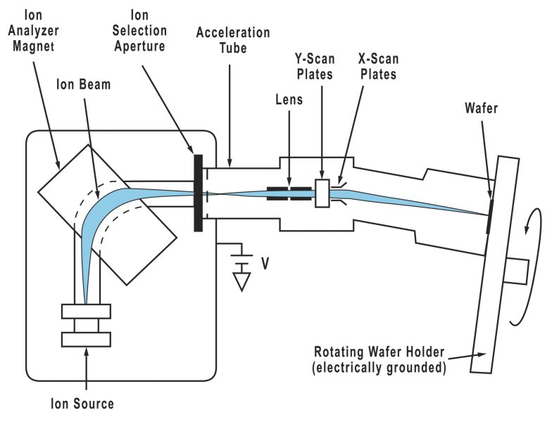
Ion implantation owes its importance to the fact that it allows precise control over the depth of penetration of dopant atoms into the silicon. In the ion implantation process, dopant atoms are first ionized in an ion source. The source typically contains a plasma, generated by either RF or microwave radiation, in which the dopant atoms are ionized by electron impact. Figure 1 shows a schematic of an ion implanter. Ion implanters must be maintained under high vacuum to permit linear free travel of the ions without occurrence of dispersion due to collisions with ambient gas molecules. Ions are extracted from the ion source using electromagnetic fields and the ion beam created by the extraction is directed into a mass analyzer where the beam is focused and bent through a right angle. The radius of the bend is determined by a combination of electromagnetic field characteristics and the mass to charge (m/e) ratio of the ions. This allows ions of a particular mass to be selected to exit the mass analyzer using a movable aperture (or an electromagnetic lens). In this way, only the desired dopant atom is selected from the different ions that may originate from the ion source. The beam of selected ions is then accelerated to high energies, ranging anywhere from sub-keV to MeV values and the high-energy ion beam is steered using electromagnetic fields so that it impinges on the semiconductor surface.
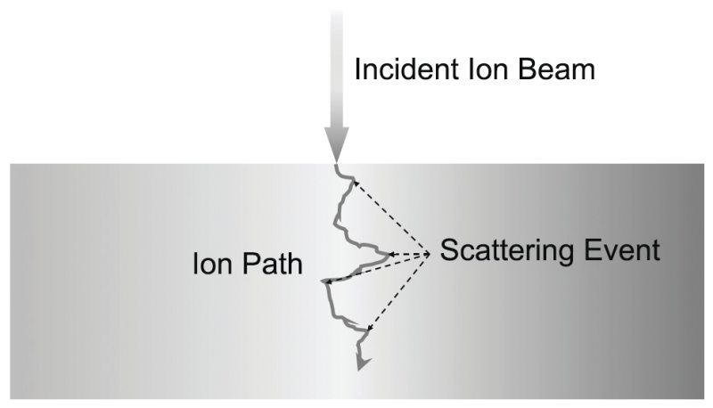
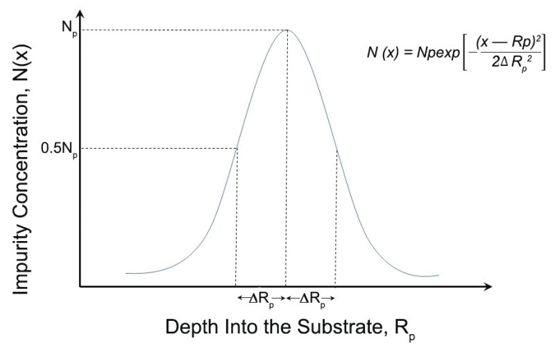
When a dopant ion strikes the substrate surface, it penetrates into the substrate crystal matrix to a depth that is proportional to its energy and angle of incidence. It doesn't penetrate the substrate in a linear manner but rather takes a "drunkard's walk" path through the crystal as its direction is scattered by collisions with substrate atoms (Figure 2). This results in a concentration profile for dopant atoms vs. penetration into the substrate that has a Gaussian distribution similar to that shown in Figure 3. Since dopant atoms do not necessarily substitute into lattice sites during the implantation process (they can come to rest in interstitial positions), post-implant annealing is necessary to "activate" the dopant by substituting the dopant atom into crystal lattice sites. The anneal will also act to repair any damage done to the silicon crystal matrix by collisions with the high-energy dopant ions and to broaden the dopant distribution profile somewhat. Once substituted into the lattice, the dopant will act as either a donor or acceptor depending on its electronic structure.
Ion implantation is normally used for n- and p-well formation in the substrate silicon and source/drain formation. The CMOS process flow discussed in Section A briefly discusses the use of ion implantation for this purpose.
Ion Implantation Products
The success of ion implantation processes is heavily dependent on the quality of the vacuum within ion implanters. As a consequence, most of MKS's product lines associated with high vacuum applications in vacuum generation, control and monitoring are of relevance in the ion implant market. Please see Vacuum Pressure Basics, Creating a Vacuum, Vacuum Measurement, and Vacuum Pressure Control for additional information. The ASTRON® Paragon® remote plasma generators can be used for F* generation in cleaning applications for ion sources and beamlines.

Related Topics
Front-end Semiconductor
For additional insights into semiconductor topics like this, download our free MKS Instruments Handbook: Semiconductor Devices & Process Technology
Request a Handbook