Chemical Mechanical Planarization
Chemical Mechanical Polishing
Chemical mechanical polishing (CMP) is a planarization technique that was developed for semiconductor applications in the late 1980s and early 1990s. During this period, the number of metal layers increased dramatically and device topographies began to exhibit features that inhibited conformal deposition and gap fill by photoresist, metal, and insulator films.
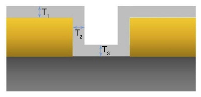
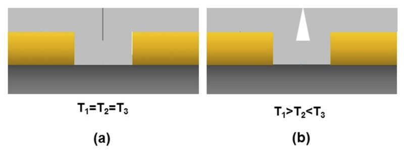
The definition of conformal deposition is demonstrated in Figure 1: a fully conformal film exhibits a ratio of 1:1 for the film thickness on planar versus vertical surfaces; i.e. T1=T2=T3. Figure 2(a) shows an idealized image of how conformal films can fill the spaces between features such as metal lines; Figure 2(b) shows how non-conformal films can result in voids in the insulating layers.
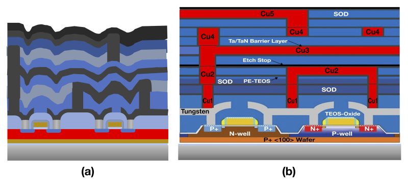
These voids are electrical weak spots that can result in device failure. As the severity of device topographies increased during the late 1980s and 1990s many variations on CVD process technology were developed that improved the conformal characteristics of insulating films and allowed their continued use. Eventually, however, the increase in the number of metal layers and more severe topographies forced device manufacturers to move to CMP as a planarization method and, within the context of semiconductor device fabrication, the acronym CMP refers to chemical mechanical planarization. Figure 3 demonstrates the difficulties encountered in fabricating a complex multi-level metal device structure using (a) non-planarized deposition technology versus (b) CMP-based planarization.
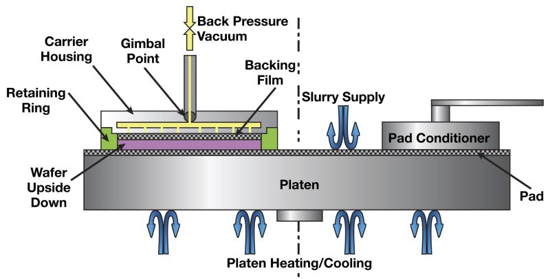
Chemical mechanical planarization, as its name implies, is a physical polishing process in which the surface of a substrate is smoothed and planarized through the combined action of chemical and physical abrasive forces on the surface. CMP combines the best of both techniques while avoiding the pitfalls. Whereas purely abrasive grinding of the surface would cause too much physical damage and purely chemical etching would not achieve planarization, the combined action of the two produces a well-planarized surface with minimal damage. Figure 4 shows a schematic of a chemical mechanical planarization tool (the image has been taken from reference. The tool consists of a rotating platen covered by a polishing pad. The wafer is mounted face down in a carrier that is pressed against the pad with a specified force. This force can be provided using either a defined and regulated gas pressure or a mechanical backing pressure system. The wafer also rotates during the polishing process. The polishing pad is saturated with a slurry of physical abrasive and chemical etchant that is pumped on to the pad. Polishing of the wafer surface occurs as the wafer is rotated on its own axis and moved about the polishing pad while being forced against the pad. During the polishing process, high points on the wafer surface are naturally subjected to more pressure and therefore more abrasive force. This combines with the action of the chemical etchant to produce an enhanced removal rate for material at the high points relative to material at low points in the surface topography. This produces the planarization effect in the process. Since heat is generated in the polishing process and changes in temperature effect etch rates, it is important to maintain a constant temperature at the pad/wafer interface during the CMP process. This is accomplished through active temperature control of the platen.
Chemical mechanical planarization has a number of advantages for semiconductor device manufacturing beyond the fact that it reduces rough topography to a planarized state. CMP allows the device manufacturer to achieve global planarization of the entire wafer surface in a single step. The approach can be used to planarize a wide range of materials, from different metals to different oxide films. It can planarize different materials in the same step (i.e., metal and insulating films). CMP is essential to the only effective method of copper patterning (damascene processing, see below). The subtractive nature of CMP helps in reducing surface defects. Finally, the process is relatively environmentally benign with no need of the hazardous gases common in dry etch processing.
Chemical mechanical planarization is employed in different planarization applications during device fabrication. Most important are oxide planarization for shallow trench isolation (STI) and Damascene processing. These applications will be described in some detail to provide practical examples of CMP.
CMP in Shallow Trench Isolation Processing
Shallow trench isolation (STI) uses trenches etched into the substrate and filled with undoped CVD polysilicon or CVD silicon dioxide as electrical isolation for the active regions in a device. It has replaced the use of thermal oxide for local oxidation of silicon (LOCOS) due to reasons related to thermal budget and the localized physical impacts of thermal oxidation of silicon. Figure 5 shows the STI process flow. Chemical mechanical polishing is used in the next to last and last steps of the STI process sequence. Following the deposition of the insulating oxide that fills the isolating trenches, CMP is used to planarize the oxide level with the nitride layer. In the last steps of the process, the nitride layer is removed followed by planarization of the CVD oxide in the trenches. STI process technology has been one of the enablers of nanometer-scale device fabrication owing to the fact that earlier LOCOS isolation schemes could not be successfully scaled down to the nanometer regime.

CMP in Damascene Processing
In the late 1980s, device speed was becoming limited by a phenomenon known as RC delays (where R is the resistance of the wiring and C is the capacitance of parasitic capacitors in the circuit structure). Signal transmission on a device is delayed in direct proportion to the resistance of the wire on which the transmission occurs and to the capacitance of any unintended capacitors formed when two metal wires are separated by an insulating material. One obvious way to reduce such delays is to reduce the R of the wiring. This prompted the replacement of aluminum (resistivity = 2.8 x 10⁻⁸ Ω-cm) wiring by copper (resistivity = 1.7 x 10⁻⁸ Ω-cm). It is noteworthy that copper also has other properties that make it preferred over aluminum as the dimensions of the wires on a device shrink (i.e., greater resistance to electromigration).
The use of copper presented serious challenges to device manufacturers. Copper cannot be etched using conventional, halide-based dry etching processes since the copper halide products are not volatile and hence cannot be pumped away by a vacuum system. This means that the conventional technology for patterning metal lines could not be used with copper. Additionally, copper does not adhere well to dielectric material and copper atoms are very mobile in SiO2. Direct deposition of copper on insulating oxide layers thus presented problems in achieving stable wiring structures and in terms of contamination of the insulating oxide (producing increased leakage).
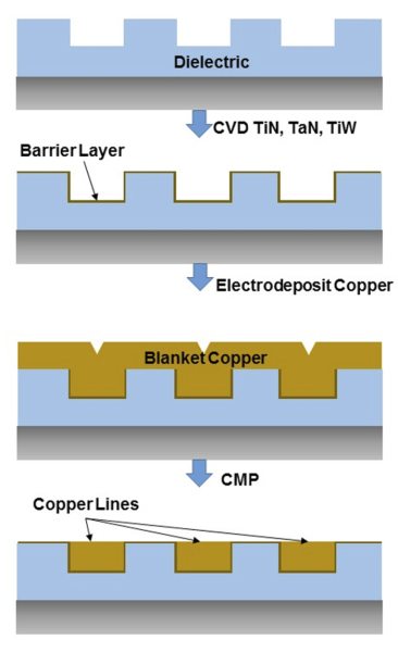
The Damascene (and Dual Damascene) process, first introduced by IBM in the early 1990s, was a unique, additive processing technique developed to address the challenges presented by the shift to copper wiring in microelectronic circuits. It gets its name from metal inlay techniques developed in Damascus in the Middle East. The process eliminates the need to dry etch copper by using chemical mechanical polishing instead and it employs special barrier layers to prevent diffusion of the copper into the oxide insulating layers. The first step in the process is the formation of the wiring pattern as etched lines in a dielectric layer (the top structure in Figure 6). A barrier layer of, for example, TiN, TaN, or TiW is then deposited on the dielectric layer to act as a barrier between the copper and the insulating dielectric. A thin seed layer of copper is deposited on the barrier, typically using PVD methods, followed by the electrodeposition of a thick copper layer. Chemical mechanical planarization is then used to remove the excess copper leaving only the metal in the etched lines behind. Several sophisticated variations on the Damascene process have been developed, but these simple steps suffice to describe the basics of how the process works.
Chemical Mechanical Planarization Products
MKS's Pressure Control products can be applied in the systems that control the backing pressure applied to the wafer holder. Pressure/Flow Controllers can be used with different MKS gas flow control valves to control the backing gas pressure on wafer carriers in CMP tools with pressures ranging from vacuum up to 100 psig.
Related Topics
Front-end Semiconductor
For additional insights into semiconductor topics like this, download our free MKS Instruments Handbook: Semiconductor Devices & Process Technology
Request a Handbook