Silicon Wafer Production
Electronic Grade Polycrystalline Silicon (Polysilicon) Purification
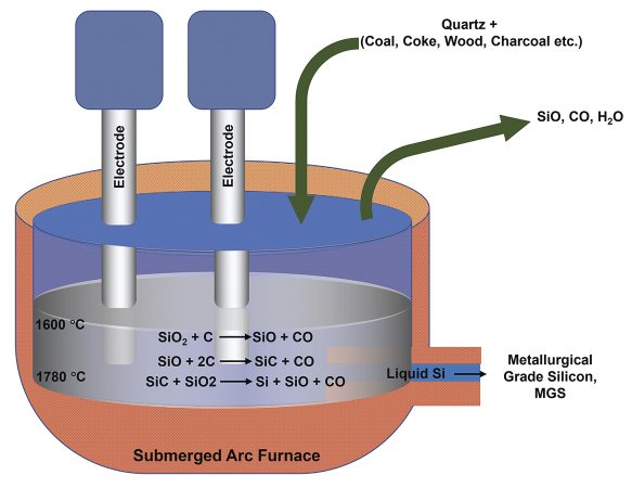
Silicon is the second most abundant element in the earth’s crust (oxygen is the first). It occurs naturally in silicate (Si-O containing) rocks and sands. The elemental silicon used in semiconductor device manufacture is produced from high purity quartz and quartzite sands, which contain relatively few impurities. Electronic grade silicon, the name used for the grade of silicon employed in semiconductor device manufacture, is the product of a chain of processes beginning with the conversion of quartz or quartzite sand to “metallurgical grade silicon” (MG-Si), in an electric arc furnace (Figure 1) according to the chemical reaction:
SiO2 + C → Si + CO2
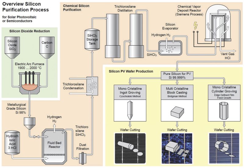
Silicon prepared in this manner is called “metallurgical grade” since most of the world’s production actually goes into steel-making. It is about 98% pure. MG-Si is not pure enough for direct use in electronics manufacturing. A small fraction (5% – 10%) of the worldwide production of MG-Si gets further purified for use in electronics manufacturing. The purification of MG-Si to semiconductor (electronic) grade silicon is a multi-step process, shown schematically in Figure 2. In this process, MG-Si is first ground in a ball-mill to produce very fine (75% < 40 µM) particles which are then fed to a Fluidized Bed Reactor (FBR). There the MG-Si reacts with anhydrous hydrochloric acid gas (HCl), at 575 K (approx. 300ºC) according to the reaction:
Si + 3HCl → SiHCl3 + H2
The hydrochlorination reaction in the FBR makes a gaseous product that is about 90% trichlorosilane (SiHCl3). The remaining 10% of the gas produced in this step is mostly tetrachlorosilane, SiCl4, with some dichlorosilane, SiH2Cl2. This gas mixture is put through a series of fractional distillations that purify the trichlorosilane and collect and re-use the tetrachlorosilane and dichlorosilane by-products. This purification process produces extremely pure trichlorosilane with major impurities in the low parts per billion range. Purified, solid polycrystalline silicon is produced from high purity trichlorosilane using a method known as “The Siemens Process.” In this process, the trichlorosilane is diluted with hydrogen and fed to a chemical vapor deposition reactor. There, the reaction conditions are adjusted so that polycrystalline silicon is deposited on electrically-heated silicon rods according to the reverse of the trichlorosilane formation reaction:
SiHCl3 + H2 → Si + 3HC
By-products from the deposition reaction (H2, HCl, SiHCl3, SiCl4 and SiH2Cl2) are captured and recycled through the trichlorosilane production and purification process as shown in Figure 2. The chemistry of the production, purification and silicon deposition processes associated with semiconductor grade silicon is more complex than this simple description. There are also a number of alternative chemistries that can be, and are, used for polysilicon production.
Single Crystal Silicon Wafer Fabrication
The silicon wafers so familiar to those of us in the semiconductor industry are actually thin slices of a large single crystal of silicon that was grown from melted electronic grade polycrystalline silicon. The process used in growing these single crystals is known as the Czochralski process after its inventor, Jan Czochralski. Figure 3 shows the basic sequence and components involved in the Czochralski process.
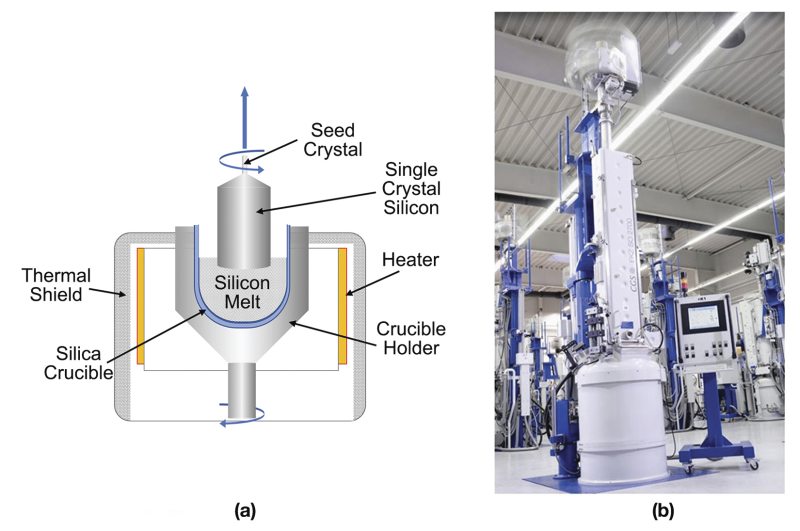
The Czochralski process is carried out in an evacuable chamber, commonly referred to as a “crystal puller” that holds a large crucible, usually quartz, and an electric heating element (Figure 3(a)). Semiconductor grade polysilicon is loaded (charged) into the crucible along with precise amounts of any dopants such as phosphorus or boron that may be needed to give the product wafers specified P or N characteristics. Evacuation removes any air from the chamber to avoid oxidation of the heated silicon during the growth process. The charged crucible is electrically heated to a temperature sufficient to melt the polysilicon (greater than 1421ºC). Once the silicon charge is fully melted, a small seed crystal, mounted on a rod, is lowered into the molten silicon. The seed crystal is typically about 5 mm in diameter and up to 300 mm long. It acts as a “starter” for the growth of the larger silicon crystal from the melt. The seed crystal is mounted on the rod with a known crystal facet vertically oriented in the melt (crystal facets are defined by “Miller Indices”). In the case of seed crystals, facets having Miller indices of <100>, <110> or <111> are typically chosen. The crystal growth from the melt will conform to this initial orientation, giving the final large single crystal a known crystal orientation. Following immersion in the melt, the seed crystal is slowly (a few cm/hour) pulled from the melt as the larger crystal grows. The pull speed determines the final diameter of the large crystal. Both the crystal and the crucible are rotated during a crystal pull to improve the homogeneity of the crystal and dopant distribution. The final large crystal is cylindrical in shape; it is called a “boule.” Czochralski growth is the most economical method for the production of silicon crystal boules suitable for producing silicon wafers for general semiconductor device fabrication (known as CZ wafers). The method can form boules large enough to produce silicon wafers up to 450 mm in diameter. However, the method has certain limitations. Since the boule is grown in a quartz (SiO2) crucible, some oxygen contamination is always present in the silicon (typically 1018 atoms cm-3 or 20 ppm). Graphite crucibles have been used to avoid this contamination, however they produce carbon impurities in the silicon, albeit at an order of magnitude lower in concentration. Both oxygen and carbon impurities lower the minority carrier diffusion length in the final silicon wafer. Dopant homogeneity in the axial and radial directions is also limited in Czochralski silicon, making it difficult to obtain wafers with resistivities greater than 100 ohm-cm.
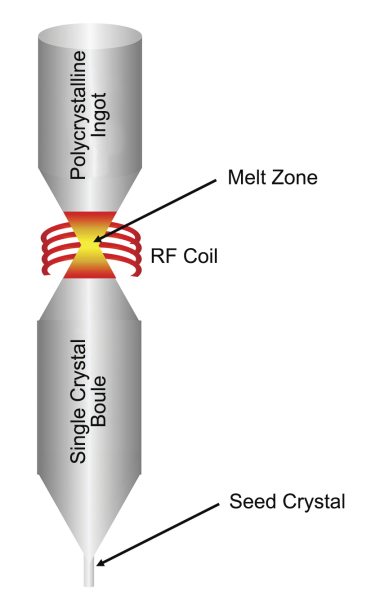
Higher purity silicon can be produced by a method known as Float Zone (FZ) refining. In this method, a polycrystalline silicon ingot is mounted vertically in the growth chamber, either under vacuum or inert atmosphere. The ingot is not in contact with any of the chamber components except for the ambient gas and a seed crystal of known orientation at its base (Figure 4). The ingot is heated using non-contact radio-frequency (RF) coils that establish a zone of melted material in the ingot, typically about 2 cm thick. In the FZ process, the rod moves vertically downward, allowing the molten zone to move up the length of the ingot, pushing impurities ahead of the melt and leaving behind highly purified single crystal silicon. FZ silicon wafers have resistivities as high as 10,000 ohm-cm.
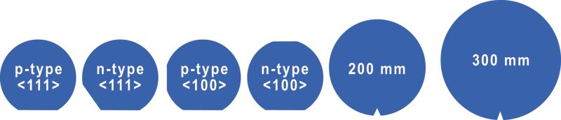
Once the silicon boule has been created, it is cut into manageable lengths and each length ground to the desired diameter. Orientation flats that indicate the silicon doping and orientation for wafers of less than 200 mm diameter are also ground into the boule at this stage. For wafers with diameters less than 200 mm, the primary (largest) flat is oriented perpendicular to a specified crystal axis such as <111> or <100> (see Figure 5). Secondary (smaller) flats indicate whether a wafer is either p-type or n-type. 200 mm (8-inch) and 300 mm (12-inch) wafers use a single notch oriented to the specified crystal axis to indicate wafer orientation with no indicator for doping type. Figure 3 shows the relationship between wafer type and the placement of flats on the wafer edge.
After the boule has been ground to the desired diameter and the flats have been created, it is cut into thin slices using either a diamond encrusted blade or a steel wire. The edges of the silicon slices are usually rounded at this stage. Laser markings designating silicon type, resistivity, manufacturer, etc. are also added near the primary flat at this time. Both surfaces of the unfinished slice are ground and lapped to bring all of the slices to within a specified thickness and flatness tolerance. Grinding brings the slice into a rough thickness and flatness tolerance after which the lapping process removes the last bit of unwanted material from the slice faces, leaving a smooth, flat, unpolished surface. Lapping typically achieves tolerances of less than 2.5 µm uniformity in wafer surface flatness.
The final stage in silicon wafer manufacture involves chemically etching away any surface layers that may have accumulated crystal damage and contamination during sawing, grinding and lapping; followed by chemical mechanical polishing (CMP) to produce a highly reflective, scratch and damage free surface on one side of the wafer. The chemical etch is accomplished using an etchant solution of hydrofluoric acid (HF) mixed with nitric and acetic acids that can dissolve silicon. In CMP, silicon slices are mounted onto a carrier and placed in a CMP machine where they undergo combined chemical and mechanical polishing. Typically, CMP employs a hard polyurethane polishing pad combined with a slurry of finely dispersed alumina or silica abrasive particles in an alkaline solution. The finished product of the CMP process is the silicon wafer that we, as users, are familiar with. It has a highly reflective, scratch and damage free surface on one side on which semiconductor devices can be fabricated.
Compound Semiconductor Wafer Production
Compound semiconductors are important materials in many military and other specialty electronics devices such as lasers, high-frequency electronic devices, LEDs, optical receivers, opto-electronic integrated circuits, etc. GaN has been commonly used in many different commercial LED applications since the 1990’s.
Table 1 provides a list of the elemental and binary (two element) compound semiconductors along with the nature of their band gap and its magnitude. In addition to the binary compound semiconductors, ternary (three element) compound semiconductors are also known and used in device fabrication. Ternary compound semiconductors include materials such as aluminum gallium arsenide, AlGaAs, indium gallium arsenide, InGaAs and indium aluminum arsenide, InAlAs. Quarternary (four element) compound semiconductors are also known and used in modern microelectronics.
The unique light-emitting ability of compound semiconductors is due to the fact that they are direct band gap semiconductors. Table 1 denotes which semiconductors possess this property. The wavelength of the light emitted by devices built from direct band gap semiconductors depends on the band gap energy. By skillfully engineering the band gap structure of composite devices built from different compound semiconductors with direct band gaps, engineers have been able to produce solid state light emitting devices that range from the lasers used in fiber optic communications to high efficiency LED light bulbs. A detailed discussion of the implications of direct versus indirect band gaps in semiconductor materials is beyond the scope of this work.
Simple, binary compound semiconductors can be prepared in bulk, and single crystal wafers are produced by processes similar to those used in silicon wafer manufacturing. GaAs, InP and other compound semiconductor ingots can be grown using either the Czochralski or Bridgman-Stockbarger method with wafers prepared in a manner similar to silicon wafer production. Surface conditioning of compound semiconductor wafers, (i.e., making them reflective and flat) is complicated by the fact that at least two elements are present and these elements can react with etchants and abrasives in different fashions.
| Material System | Name | Formula | Energy Gap (eV) | Band Type(I = indirect; D = direct) |
|---|---|---|---|---|
| IV | Diamond | C | 5.47 | I |
| Silicon | Si | 1.124 | I | |
| Germanium | Ge | 0.66 | I | |
| Grey Tin | Sn | 0.08 | D | |
| IV-IV | Silicon Carbide | SiC | 2.996 | I |
| Silicon-Germanium | SixGe1-x | Var. | I | |
| IIV-V | Lead Sulfide | PbS | 0.41 | D |
| Lead Selenide | PbSe | 0.27 | D | |
| Lead Telluride | PbTe | 0.31 | D | |
| III-V | Aluminum Nitride | AlN | 6.2 | I |
| Aluminum Phosphide | AlP | 2.43 | I | |
| Aluminum Arsenide | AlAs | 2.17 | I | |
| Aluminum Antimonide | AlSb | 1.58 | I | |
| Gallium Nitride | GaN | 3.36 | D | |
| Gallium Phosphide | GaP | 2.26 | I | |
| Gallium Arsenide | GaAs | 1.42 | D | |
| Gallium Antimonide | GaSb | 0.72 | D | |
| Indium Nitride | InN | 0.7 | D | |
| Indium Phosphide | InP | 1.35 | D | |
| Indium Arsenide | InAs | 0.36 | D | |
| Indium Antimonide | InSb | 0.17 | D | |
| II-VI | Zinc Sulfide | ZnS | 3.68 | D |
| Zinc Selenide | ZnSe | 2.71 | D | |
| Zinc Telluride | ZnTe | 2.26 | D | |
| Cadmium Sulfide | CdS | 2.42 | D | |
| Cadmium Selenide | CdSe | 1.70 | D | |
| Cadmium Telluride | CdTe | 1.56 | D |
Table 1. The elemental semiconductors and the binary compound semiconductors.
Related Topics
Front-end Semiconductor

For additional insights into semiconductor topics like this, download our free MKS Instruments Handbook: Semiconductor Devices & Process Technology
Request a Handbook