Semiconductor Fab Utilities Overview
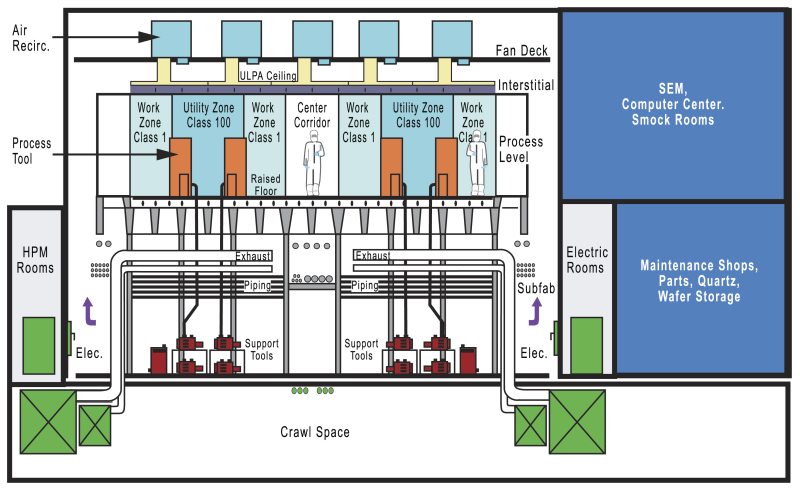
For many of us, our direct experience with the reality of a semiconductor fabrication facility is limited to meeting rooms, cleanrooms and analytical laboratories. These facilities are, however, part of much more complex structures that contain an intricate infrastructure of ancillary environments housing regulatory, production and delivery systems for the different services and utilities needed for day-to-day fab operation. Figure 1 is a layout diagram for a typical semiconductor fab that shows the ancillary areas needed to provide utility services to the cleanroom production zone. These services include ultrapure water, bulk high purity gases such as nitrogen and argon, exhaust gas handling and disposal, and cleanroom air systems. This section discusses these fab utility systems and supplies context for how different products in MKS's portfolio are employed in these areas. Also, while many of the references in this section are to 200 mm wafer processing, the subject matter is generally applicable to 300 mm wafer processing as well.
Ultrapure Water
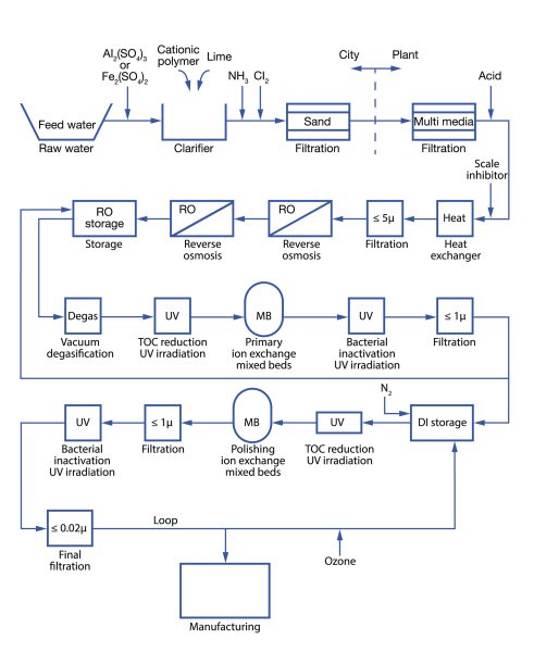
Ultrapure water is required for many semiconductor process steps. Early stages of device fabrication require repeated steps for wafer cleaning, rinsing and surface conditioning. At many different stages in device manufacturing, it is used for surface cleaning, wet etch, solvent processing, and chemical mechanical planarization. Indeed, the latter unit process has become one of the largest consumers of UPW within the fab, requiring high volumes for slurry production and rinsing. Please see Ultrapure Water for Semiconductor Manufacturing for additional information.
Gas Storage and Delivery
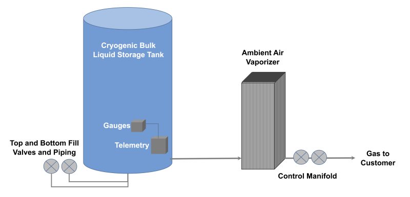
All of the gases used in a semiconductor device manufacturing plant must be of extremely high purity at their source and this purity must be maintained throughout the gas distribution systems that exist within the plant. Some gases may also require further point of use (POU) purification to ensure ultra-low contaminant levels in critical processes. Please see Semiconductor Gas Storage and Delivery for additional information.
Exhaust Gas Treatment
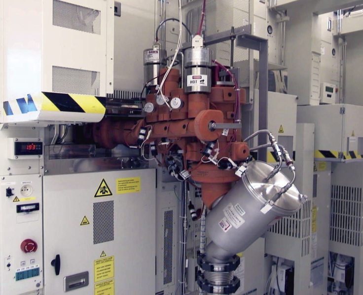
The process exhaust downstream from the cleaning, deposition and metal etch processes employed in a semiconductor fab often experiences problems due to fouling. This is most often caused by the condensation and build-up of solid or liquid process by-products on the internal surfaces of vacuum components and exhaust lines. Such build-up can be controlled by maintaining the exposed surfaces at elevated temperatures; therefore fabs require technologies that accurately and precisely control the surface temperatures of the different components in the vacuum train and exhaust gas handling systems. Exhaust streams in a fab frequently contain very corrosive and/or toxic gases that must be removed by chemical scrubbing prior to release to the atmosphere. This entails the use of equipment in most fabs that is dedicated to managing and treating the process exhaust gas stream. Please see Semiconductor Exhaust Gas Treatment for additional information.
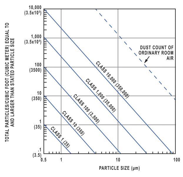
Cleanroom Ultra-clean Air Delivery
Semiconductor fab environments require ultra-clean conditions to ensure low numbers of product defects due to particulate contamination. A critical aspect in creating an ultra-clean environment is proper design of an air purification and handling system to deliver ultra-low particulate air to the work environment. Please see Cleanroom Ultra-clean Air Delivery for additional information.
Related Topics
Semiconductor Fab Utilities
- Ultrapure Water for Semiconductor Manufacturing
- Semiconductor Gas Storage and Delivery
- Semiconductor Exhaust Gas Treatment
- Cleanroom Ultra-clean Air Delivery
Front-end Semiconductor
For additional insights into semiconductor topics like this, download our free MKS Instruments Handbook: Semiconductor Devices & Process Technology
Request a Handbook