
Semiconductor Inspection
Solutions for Inspecting the Smallest Semiconductor Feature Sizes
The progression to ever smaller feature sizes on both substrates and mask/reticles produces lower and lower tolerance to defects in both starting materials and finished devices. Not only are we approaching near zero tolerances to known defect types (particles, crystal defects, etc.), but manufacturers continue to discover device sensitivities to entirely new types of defects as manufacturing progresses into the deep nano-scale. In addition, the available metrologies for defect detection are being required to sense and quantify defects at very near the noise level of their operating principles and new approaches to defect detection are continually being developed.
Unpatterned Wafer Inspection
Historically, device manufacturers have used optical detection systems to inspect wafers and masks for the presence of particles and other types of defects. Modern wafer inspection tools detect particles and pattern defects and determine the position of these defects in an X-Y grid on the wafer which can be output to the user for diagnostic purposes.

Bare substrate wafers are typically inspected when shipped from the wafer manufacturer and on receipt by device manufacturers. Bare or unpatterned wafers may also be monitored before and after being subjected to a passive or active process environment in order to determine a baseline for particle contributions from a given process. The basic principle used for defect detection on unpatterned wafers is relatively simple. A laser beam is radially scanned over the surface of a rotating wafer to ensure that the beam is projected onto all parts of the wafer surface. The laser light is reflected from the surface as it would be from a mirror. When the laser beam encounters a particle or other defect on the surface of the wafer, the defect scatters a portion of the laser light. Depending on the illumination arrangement, the scattered light can be detected either directly (dark-field illumination) or as a loss in intensity in the reflected light beam (bright-field illumination).
Patterned Wafer Inspection
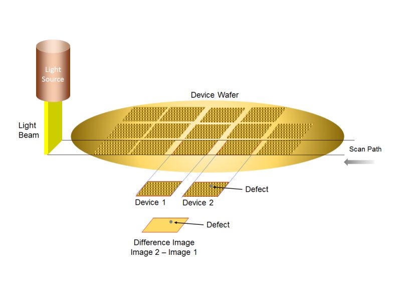
Optical inspection of patterned wafers can employ bright-field, dark-field illumination or a combination of both for defect detection. Additionally, electron beam (EB) imaging is also used for defect inspection, especially at smaller geometries where optical imaging is less effective. However, it is very slow and only used at the R&D stage. Patterned wafer inspection systems employ a comparative method in which they image a given die on the wafer and compare that image with the image of an adjacent die or that of a “golden” die known to be defect free. Inspection tools use image processing software to subtract one image from the other and if there is a random defect in one of the die, it will not zero out in the subtraction process, showing up clearly in the subtracted image. The position of the defect is defined in terms of the position within the die and the die position on the wafer allowing a defect map to be generated over the wafer, similar to that generated with unpatterned wafers.
Reticle Inspection
Arguably, reticle inspection is far more important than either non-patterned or patterned wafer inspection. This is due the fact that, while a single defect on a bare or patterned wafer has the potential to “kill” one device, a single defect on a reticle can destroy thousands of devices (or more!) since that defect is replicated on every wafer processed using that particular reticle.
Reticle inspection systems work on the same basic principles and have similar physical requirements to wafer inspection tools, with the exception that reticles are typically inspected using transmitted, rather than, reflected light. Reticle inspection tools employ high resolution imaging optics and either conventional visual or UV wavelength illumination, depending on defect tolerances and/or feature sizes, to find defects on a reticle blank or a patterned reticle. Inspections are routinely performed during both the reticle manufacturing process and throughout the reticle use phase. Reticle inspection tools employ image analysis software algorithms and motion control systems similar to wafer inspection tools. Using UV illumination, the application of conventional optical reticle inspection systems has been extended down to the 90-nm feature sizes; for smaller features, electron beam, EB, reticle inspection is used.
Inspection and Metrology Solutions
Motion Control for Wafer Inspection
We offer a variety of high performance air bearing stages suitable for use in wafer inspection tools and other motion control applications. The HybrYX™ XY Hybrid Air Bearing XY Stage is a relatively low cost, single plane air bearing stage that is well suited for semiconductor wafer inspection systems and many other scanning applications requiring ultra-low velocity ripple & dynamic following error. The HybrYX stage has a true single place XY architecture with available theta and Z-Tip-Tilt solutions. It features scanning velocities of up to 600 mm/sec and 0.6G acceleration and large (>1 meter) XY Travel range The HybrYX system has a demonstrated and reliable, long-life operation ideal for high duty cycle environments such as wafer inspection applications.
The DynamYX® family of reticle positioning stages were specifically designed for semiconductor wafer processing and inspection applications. They offer the highest level of commercially available positioning performance. The extensive use of ceramic materials in these stages provides exceptionally rigid structural stability. They are designed with a low profile that aids in OEM applications.
Motion Control for Reticle Inspection
The DynamYX Reticle Positioning Air Bearing Stage is designed for use in reticle inspection and repair applications. The DynamYX stage has a much smaller footprint than traditional open-frame solutions and a full-openaperture that accommodates flexible optical component integration and ease of service access.
Custom Optical Solutions
We offer optical sub-system design and manufacturing solutions for wafer and reticle
inspection tool manufacturers. We have designed and manufactured optical sub-systems for lithography, wafer inspection, excimer and EUV light source, metrology and mask writing applications, among others.
Semiconductor Devices and Process Technology Handbook
For additional information on semiconductor inspection and metrology as well as other semiconductor applications please download our free Semiconductor Devices and Process Technology eBook.


