Semiconductor Lithography Solutions
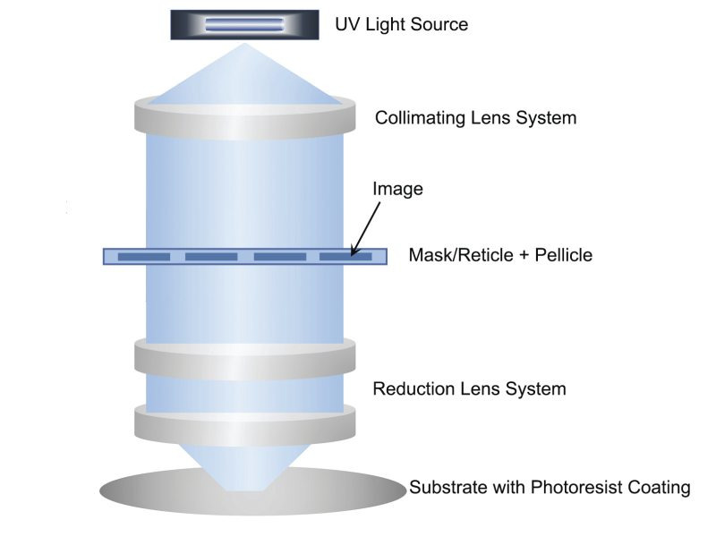
As the demand for reducing the size of transistors on a semiconductor chip increases, photolithography is the technique of choice for patterning in semiconductor device manufacturing because it is optical, enabling small features and high wafer throughput.
MKS solutions for enhancing semiconductor lithography include high-performance air bearing stage products suitable for use in semiconductor photolithography applications and customized tools for automated manufacturing and process control.
Learn More:
MKS Handbook Second Edition
Semiconductor Devices and Process Technology
Detailing the fundamental device physics, materials, and fabrication processes used to manufacture semiconductors.
A free book from MKS

MKS Handbook
Principles & Applications in Photonics Technologies
The enabling technology for fiber optic communications, bioimaging, laser surgery, LED lighting, security, flexible electronics, wafer inspection & metrology, and lithography for semiconductor device manufacturing.
A free book from MKS
Diffraction Grating Handbook
A primary source of information regarding diffraction gratings used in the lithography process
IR Long Range Zoom Lenses
An extensive collection of long range zoom lenses for a wide range of applications, including semiconductor photolithography
Diffraction Gratings
Newport offers precision components for semiconductor lithography
Semiconductor Photolithography
A detailed discussion of the photolithography process used in semiconductor manufacturing
Motion Control
An extensive catalog of manual positioning and motion control standard and custom products enhancing photolithography processing.
Optical Filters
A full spectrum of solutions for managing light sources
Optics and Optical Components
Competitively priced high performance optics to optimize semiconductor manufacturing
Air Bearing Stages for Lithography Applications
High performance air bearing stage solutions for semiconductor lithography applications.
Ophir Laser Optics
A full range of high quality OEM and replacement optics for high power CO2 laser and 1μm laser applications