Reactive Ion Etching
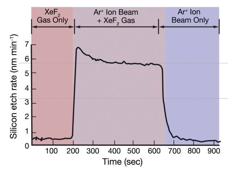
Reactive Ion Etching (RIE) uses a combination of chemical and physical reactions to remove material from a substrate; it is the simplest process that is capable of directional etching. A highly anisotropic etching process can be achieved in RIE through the application of energetic ion bombardment of the substrate during the plasma chemical etch. The RIE process thus provides the benefits of highly anisotropic etching due to the directionality of the ions bombarding the substrate surface as they get accelerated towards the negatively biased substrate, combined with high etch rates due to the chemical activity of the reactive species concurrently impinging on the substrate surfaces. The synergistic effect of ion bombardment on increased etch rates in the presence of chemically active species was first demonstrated and explained by Coburn and Winters, where they showed the significantly higher silicon etch rate in the presence of both Ar+ ion beam and XeF2 gas compared to either the Ar+ ion beam or the XeF2 gas only as illustrated in Figure 1. In the RIE process, the ions carry sufficient energy to break the chemical bonds of the atoms in the substrate that they impinge upon lowering the activation energy for the chemical etching reactions and thus increasing the reaction rates with the reactive neutrals that are also incident on the substrate surface. In certain etching chemistries, there may be reaction byproducts that are formed on the surface and act as inhibitors for the chemical etch processes. The energetic ions also act to remove such reaction byproducts from the surface through physical sputtering exposing the underlying material to be removed by the chemically reactive species. Thus RIE is sometimes also referred as Ion-Enhanced Etching or Reactive and Ion Etching. The highly directional nature of ions bombarding the surfaces leads to the anisotropy in the etch process as illustrated in the Figure 2.
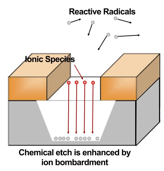
As the ions are incident perpendicular to the surface, the etch rate is significantly enhanced in the vertical direction as the ions largely interact with the bottom surface of the trench being etched activating the surface and removing any reaction inhibiting byproducts preferentially from the bottom surface while the deposits/byproducts on the sidewalls act to prevent/minimize the chemical etch from the sidewalls leading to near vertical etch profiles. This high degree of anisotropy is critical in the definition of closely spaced (fine pitch) features in semiconductor manufacturing and is critical in scaling the device features to ever-shrinking dimensions in accordance with Moore's law. The degree of anisotropy in RIE is directly related to the balance between the energy and angular distribution of the incident ion flux and the passivation properties of the reaction byproducts. The incident ion energy and angular distribution is directly related to the electric field drawing the ions towards the substrate and the number of collisions these ions may encounter as they impinge towards the substrate through the accelerating field (function of pressure). Lower pressure and higher substrate bias are key factors that control the ion energy (increase) and angular distribution (reduce) while the polymer formation is largely a function of the polymer forming (CxFy) precursor partial pressure used as one of the etchant gases.
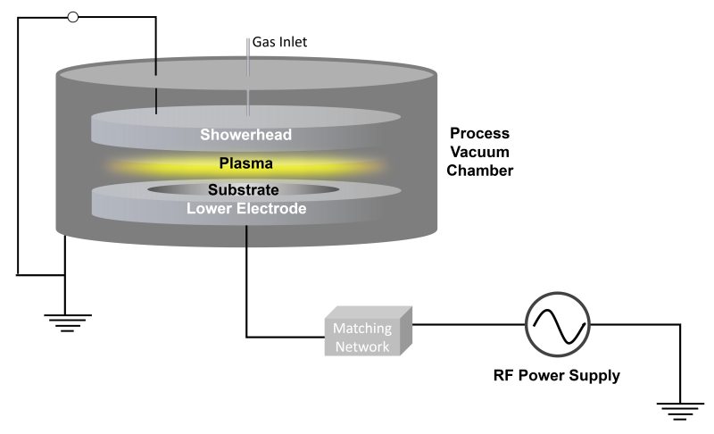
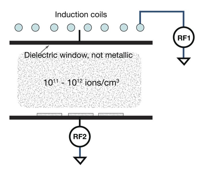
Figure 3 shows a schematic for a typical RIE plasma chamber. RF power is used to excite the plasma and the substrate being processed sits on a powered electrode. The powered electrode enhances the negative bias on the substrate, promoting ion acceleration and surface bombardment. The accelerating voltages experienced by ions in an RIE process are significantly lower than those employed for physical etching processes, producing a much lower potential for substrate damage. Ion energies in RIE are typically between 1 and 30 eV as compared to energies well in excess of 300 eV commonly employed for Physical Vapor Deposition (PVD) approaches. One of the key challenges with such an RIE system is that the same power supply generates the plasma as well as pulls the ions towards the substrate being processed. This configuration is thus limited to capacitively coupled plasmas that typically operate between 10-100 mTorr pressure. For higher etch rates as well as additional process flexibility, inductively coupled plasma sources are used wherein the plasma generation is controlled through a separate RF power supply while the substrate is biased through a second RF supply. Such a system is shown in Figure 4 where the inductively coupled high density plasma is controlled through the first RF power supply (RF1) while the substrate bias is controlled through an independent power supply (RF2). This configuration can enable additional functionality such as modulated pulsed bias as well as operation at lower pressures <10mT for improved etch uniformity across the semiconductor substrates. The pulsing function is especially useful in addressing the issue of Aspect Ratio Dependent Etch (ARDE), wherein the smaller feature structures (higher aspect ratio) etch at a lower rate than the wider features on the same substrate under the same process conditions due to a slower rate of removal/diffusion of the reaction products from high aspect ratio/narrow features. MKS has developed RF generators with unique pulsing capabilities to address these process challenges for semiconductors OEMs manufacturing such HDP etch systems.
Related Topics
Semiconductor Etching
For additional insights into semiconductor topics like this, download our free MKS Instruments Handbook: Semiconductor Devices & Process Technology
Request a Handbook