FinFET Physics
As MOSFET devices have continued to shrink in size, certain limitations have begun to impact their performance. Specifically, at nanometer dimensions, subthreshold current leakage becomes a significant factor (Ioff becomes unacceptably high) and the potential on the drain begins to dominate the electrostatics in the channel region of the device. This causes a loss of gate control over the device current and an increase in Ioff; these characteristics are known as short channel effects. Increases in Ioff have obvious consequences for device performance. The problem especially impacts the devices used in mobile applications where it can lead to an unacceptable drain on battery power. Over the years, this problem has been overcome through the use of ever thinner gate oxides and the deployment of high-k dielectric materials that increase the gate-channel capacitance. These approaches have been effective up to about a decade or so ago when the continued thinning of gate oxides produced irremediable problems with gate leakage and gate-induced drain leakage in nanometer-scale devices. These problems have been resolved through the use of an approach known as multi-gate FETs (MGFETs), a three-dimensional departure from traditional planar MOSFET designs.
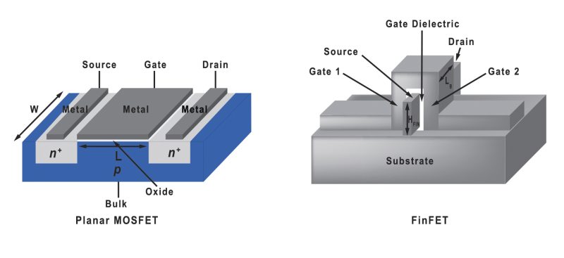
Currently, the dominant non-planar transistor device geometry is the Fin Field Effect Transistor or FinFET. Figure 1 shows a comparison between the structure of a conventional planar MOSFET and that of a FinFET. It can be seen that all of the familiar components of a MOS device are present in the FinFET (drain, source, gate, gate dielectric) and that the device more effectively separates the source and drain from the substrate silicon (FinFETs can be constructed on both bulk silicon and on buried oxide layers) and has a multiple gate configuration. The source and drain regions are now part of a vertical fin structure with the gate dielectric and gate electrode wrapped around it to produce multiple gates, one on either side of the fin as well as one on top of the device. FinFETs can also be extended to create a gate all around the device.
FinFET designs produce much better control of the gate current by using more than one gate to control a single channel. They have much lower Ioff leakage characteristics and can conduct significantly more current in the On state than comparable MOSFET designs.
Related Topics
Semiconductor Physics
Basic Device Structures

For additional insights into semiconductor topics like this, download our free MKS Instruments Handbook: Semiconductor Devices & Process Technology
Request a Handbook