Single Crystal Silicon Wafer Manufacturing
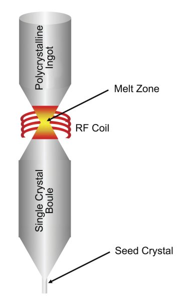
Higher purity silicon can be produced by a method known as Float Zone (FZ) refining. In this method, a polycrystalline silicon ingot is mounted vertically in the growth chamber, either under vacuum or inert atmosphere. The ingot is not in contact with any of the chamber components except for the ambient gas and a seed crystal of known orientation at its base (Figure 2). The ingot is heated using non-contact radio-frequency (RF) coils that establish a zone of melted material in the ingot, typically about 2 cm thick. In the FZ process, the rod moves vertically downward, allowing the molten zone to move up the length of the ingot, pushing impurities ahead of the melt and leaving behind highly purified single crystal silicon. FZ silicon wafers have resistivities as high as 10,000 ohm-cm.
The final stage in silicon wafer manufacture involves chemically etching away any surface layers that may have accumulated crystal damage and contamination during sawing, grinding and lapping; followed by chemical mechanical polishing (CMP) to produce a highly reflective, scratch and damage free surface on one side of the wafer. The chemical etch is accomplished using an etchant solution of hydrofluoric acid (HF) mixed with nitric and acetic acids that can dissolve silicon. In CMP, silicon slices are mounted onto a carrier and placed in a CMP machine where they undergo combined chemical and mechanical polishing. Typically, CMP employs a hard polyurethane polishing pad combined with a slurry of finely dispersed alumina or silica abrasive particles in an alkaline solution. The finished product of the CMP process is the silicon wafer that we, as users, are familiar with. It has a highly reflective, scratch and damage free surface on one side on which semiconductor devices can be fabricated.
For additional insights into semiconductor topics like this, download our free MKS Instruments Handbook: Semiconductor Devices & Process Technology
Request a Handbook