Orientation by Design: Precision Nanostructure Alignment for Advanced Packaging
Overview
For engineers designing next-generation electronic packages, precise control over material properties is essential to meet aggressive thermal, electrical, and reliability targets. Traditional isotropic materials often fall short. MKS introduces microwave-assisted nanostructure alignment, a manufacturing technique that integrates engineered anisotropy directly into high-volume production lines.
This process enables faster cycles, tighter uniformity, and materials intentionally optimized for performance through controlled pathway alignment (conductivity, heat spreading, and RF behavior, on purpose).
Where Does Engineered Anisotropy Move the Needle in Semiconductors?
Microwave-assisted alignment provides targeted solutions across critical semiconductor applications:
- Thermal Interface Materials (TIMs) and Mold Compounds: Align graphene/hex-BN platelets to create efficient in-plane heat spreaders. This effectively mitigates hotspots across complex architectures like stacked memory or 2.5D interposers.
- EMI/EMC Shielding & Conductive Adhesives: Orient CNT/metal nanowire networks to achieve target sheet resistance with significantly lower filler loading. The result is thinner films, reduced warpage, and cleaner deposition windows crucial for RF front-end modules and advanced System-in-Package (SiP) designs.
- Underfill & Encapsulation Reliability: Controlled alignment within polymer matrices improves stress distribution and enhances reflow stability. This is vital for maintaining dimensional control in demanding panel-level packaging processes.
- Optical/RF Layers in Advanced Modules: Directional alignment of nanoplatelets/nanowires precisely tunes anisotropic absorption/reflection properties, ensuring consistent filtering and shielding performance across all production lots.
Why Do Microwaves Change the Scale-Up Equation?
Microwave technology fundamentally alters how nanostructures interact with their environment during processing, translating laboratory success into repeatable, high-volume manufacturing yield:
- Volumetric, Selective Heating: Ensures uniform thermal profiles across panels or wafers in minutes, rather than hours, which minimizes warpage risks.
- Field–Matter Coupling: The microwave electric field induces dipolar polarization, actively assisting the physical alignment of nanostructures precisely when the polymer matrix reaches optimal process viscosity.
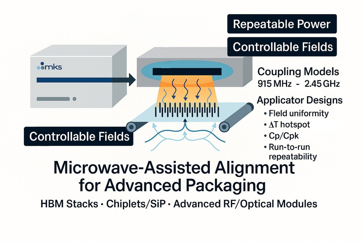
- Inline Control: Integrated power, temperature, and reflected-power diagnostics convert the alignment process from a variable into a repeatable, controllable manufacturing step.
Why MKS Wins: From Pilot to High-Volume Manufacturing
MKS provides the reliable, scalable microwave subsystems necessary for advanced packaging applications.
| Feature | Engineering Benefit |
|---|---|
| Spectral Purity & Frequency Stability | Clean, stable output provides predictable coupling, uniform heating, and consistent alignment run after run. |
| Reliability | Precise ramping and tight control loops are built for industrial duty cycles, ensuring process repeatability. |
| Closed-Loop Matching | Real-time impedance management minimizes hotspots and protects the process window on sensitive panels, laminates, or molded parts. |
| Applicator + Process Co‑Design | We partner on custom applicator geometry, fixtures, and recipes tailored to specific materials (CNT, BN, graphene, nanowires) and package architectures (fan-out, 2.5D/3D, SiP). |
| Factory Integration | Interlocks, recipe management, traceability, and safety systems designed for cleanroom-ready deployments. |
| Global Support | Applications and service coverage in Europe, the U.S., and Asia de-risks commissioning and production ramp. |
MKS Microwave Solutions?
MKS provides a comprehensive range of industrial microwave generators: 915 MHz up to 100 kW and beyond, and 2.45 GHz up to 15 kW.
Contact MKS today to engineer anisotropy into your advanced packaging processes.